PDF

Importing PCBs — Using the Add-In
Introduction
This tutorial series demonstrates how to import printed circuit board (PCB) data from the IPC-2581 file format and generate simulation-ready geometry. Key topics include selecting the import type, handling drill layers, creating simplified 3D components and pads, and previewing file content before importing. The tutorials also show how to remove small details, such as short edges, either through Automatic Geometry Cleanup or by simplifying and repairing geometry during import. Geometry finalization is done using Form Union or Form Assembly, followed by mesh generation with adjusted element sizes to resolve small copper trace features using the Free Tetrahedral and Swept mesh generators.
This tutorial, the fourth in the series, uses the PCB to Material data add-in to prepare a PCB for simulation by replacing its detailed internal structure with a space-dependent interpolation function for the material properties. The model also considers the influence of thermal expansion caused by the heat dissipation from several resistors placed on the board.
The first tutorial in the series, Importing PCBs — Generating Shell Traces, shows how to model copper traces as shell geometry, automatically remove small details with Automatic Geometry Cleanup, and use import-generated selections to assign materials.
The second tutorial, Importing PCBs — Creating Component Domains, demonstrates how to import PCBs with extruded copper traces, simplify and repair geometry during import, and create pads for simplified components. The geometry is finalized with Form Assembly and meshed using the Swept operation.
The third tutorial, Importing PCBs — Working with Nets, shows how to use the 2D Preview to selectively import nets and prepare a simplified geometry. It also demonstrates how to partition the board geometry with a bounding box for selected nets.
Model Definition
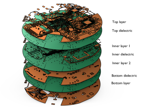
The IPC-2581 file imported in this tutorial contains a PCB with four copper layers connected by vias.
This model uses the PCB to Material Data add-in available from the Add-in Libraries with the ECAD Import module. Instead of explicitly modeling every trace and via in the geometry, the add-in creates an interpolation function that captures the different material properties across the board. A resulting simplified geometry is then generated by extruding the PCB outline according to the layer stackup defined in the input file. With the user interfaces provided by the add-in, you can choose the material properties for the traces, dielectric regions, and via cores, and select the components to include in the model. In this tutorial, the simplified domains of a few resistors are generated to study the heat dissipation across the board. For the physics setup, assume that a resistor dissipates 62.5 mW of power as heat. Conduction to the PCB and convection to the surrounding air provide cooling. All boundaries are cooled with a heat transfer coefficient of 5 W/(m2·K) that corresponds to natural convection. The thermal conductivities are chosen to be similar to:
The displacements in the Solid Mechanics interface are constrained in such way that the PCB can freely deform while its rigid body motions are suppressed.
The PCB to Material Data Add-In
The settings window for the add-in is used to select the PCB file and to configure the import. First, you can review the layers to consider for the analysis, and if necessary change the layer names and thicknesses. The material properties for skipped copper layers will be replaced with dielectric material properties in the interpolation file. At least one copper or dielectric layer with nonzero thickness needs to be selected for the import.
Next, you can choose the materials for the metal and dielectric layers and the via cores. The default choices are copper for the metal domains and FR4 for the dielectric domains. You can also select custom materials defined under the global Materials node in the model. Make sure that the materials contain at least the following six material properties: heat capacity, density, thermal conductivity, Young’s modulus, Poisson’s ratio, and coefficient of thermal expansion. These properties are necessary for simulations involving heat transfer, solid mechanics, and thermal stress. Note that only constant values are supported.
Once run, the add-in starts with determining an appropriate interpolation grid size that is selected to correspond to the radius of the smallest via in the PCB. If no valid drill layers can be found in the file, a grid size will instead be estimated based on the bounding box of the PCB.
The add-in then processes metal and dielectric layers, evaluating for each layer the material properties on the generated grid, and storing the property values in the file that will be used as input for the interpolation function added later. The interpolation data is written using a grid file format, where the first section of the file defines a regular grid - points inside the PCB volume where the material data is evaluated. The second section contains the material property values. You can easily reuse the interpolation data in other models by creating a copy of the generated file, which you can find in the folder for user files specified under Preferences > Files > Folder for user files.
Interpolation Function
When the processing of the PCB file is complete, an Interpolation feature, inserted under the Definitions branch of the target Component, is used to load the generated file. Another possibility for creating a copy of the interpolation data is by clicking Export from the settings for the interpolation feature.
The interpolation and extrapolation settings determine how values are evaluated between grid points and outside the defined coordinate domain. By default, both use Nearest neighbor, which preserves the discrete layer transitions. You can select one of the other available alternatives to interpolate between points where material property values are defined.
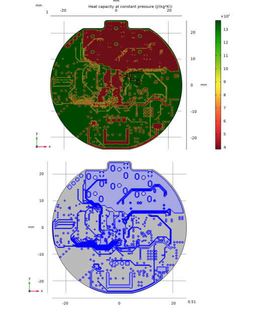
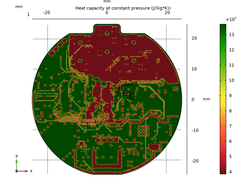
Figure 1: Material properties of the board (top), geometry (bottom) of the inner layer 1.
The heat capacity evaluated at the elevation of the inner layer 1 using the interpolation function set up by the add-in can be compared to the geometry generated for the layer in Figure 1.
Simplified Geometry and Meshing
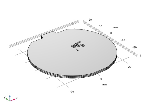
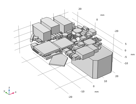
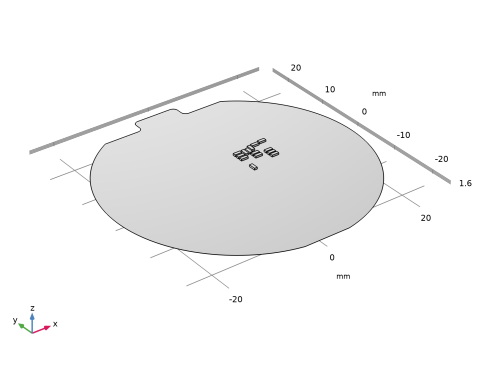
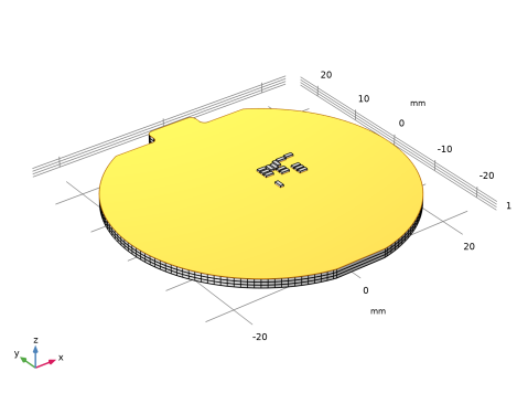
To generate a simplified PCB geometry, the outline of the board is extruded to match the layer elevations. The geometric domains for the selected components are also created at this stage. Finally, a mesh is generated using the quad and swept mesh generators. The mesh element size is determined based on the interpolation grid size.
The PCB featured in this tutorial originates from OtterCastAudioV2, Copyright © 2024 Ottercast, Jana Marie Hemsing, and it is made available under the MIT license.
Results and Discussions
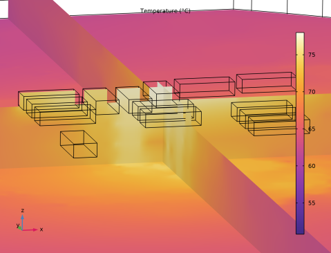
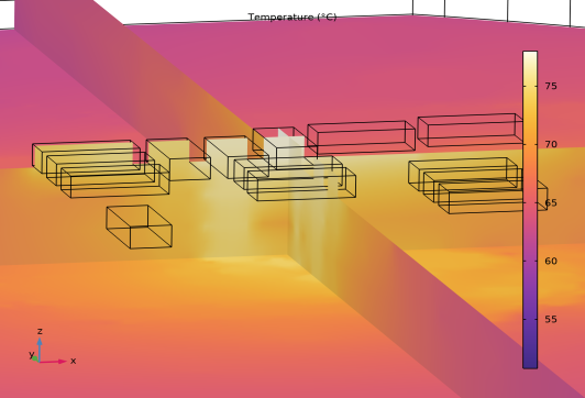
Figure 2 illustrates the temperature distribution inside the PCB.
Figure 2: Multislice plot of the temperature distribution in the PCB close to heat dissipating components.
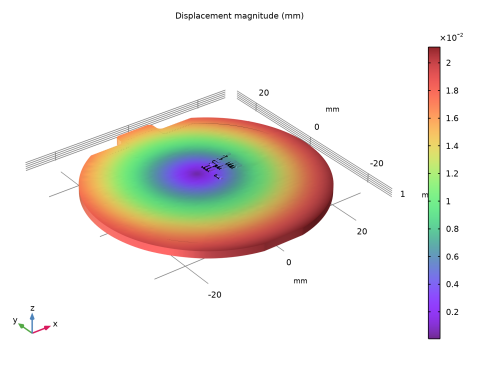
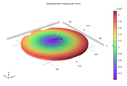
Figure 3 shows the displacement magnitude due to thermal expansion.
Figure 3: Magnitude of displacement in the PCB (exaggerated by a factor of 160).
Application Library path: ECAD_Import_Module/Tutorials/pcb_import_addin
Modeling Instructions
From the File menu, choose New.
New
In the New window, click  Model Wizard.
Model Wizard
1
In the Model Wizard window, click  3D.
2
In the Select Physics tree, select Structural Mechanics > Thermal–Structure Interaction > Thermal Stress, Solid.
3
Click Add.
4
Click  Study.
5
In the Select Study tree, select General Studies > Stationary.
6
Add Material
Start by adding materials to the Global Materials that will be used to define material properties of the PCB.
1
In the Home toolbar, click  Add Material to open the Add Material window.
2
Go to the Add Material window.
3
In the tree, select Built-in > Copper and Built-in > FR4 (Circuit Board).
4
Click the Add to Global Materials button in the window toolbar.
5
In the Home toolbar, click  Add Material to close the Add Material window.
Global Definitions
FR4 (Circuit Board) (mat2)
In the Home toolbar, click  Windows and choose Add-in Libraries.
Add-in Libraries
1
In the Add-in Libraries window, in the tree, select the checkbox for the node ECAD Import Module > pcb_to_material_data.
2
3
In the Developer toolbar, click  Add-ins and choose PCB to Material Data > PCB to Material Data.
PCB to Material Data
1
In the Model Builder window, under Global Definitions click PCB to Material Data.
2
In the Settings window for PCB to Material Data, locate the Source section.
3
Click Browse.
4
5
Locate the Layers section.
The table contains the layer stackup for the PCB, including only the metal, dielectric and drill layers. By default, all layers are selected to be processed by the add-in.
6
Locate the Target section.
Here you can choose where the interpolation function and the simplified geometry will be created. By default, the add-in inserts them in a new 3D component. Alternatively, you can select an already existing 3D component.
7
From the Component list, choose Component 1 (comp1).
8
Locate the Materials section.
You can assign different materials for metal and dielectric layers of the PCB. By default, copper is assigned for metal and FR4 for dielectric material. You can use other materials, like composite epoxy materials, metal-core substrates or specialized copper composites defined under Global Materials. Note that each material must provide six constant values, see The PCB to Material Data Add-In.
9
From the Metal list, choose From Global materials.
10
11
From the Dielectric list, choose From Global materials.
12
From the list, choose FR4 (Circuit Board).
13
Locate the Vias section.
In this section you can choose the material properties for the via cores and optionally their plating. By default, via cores are defined by copper material properties, but you can also choose between FR4 or a user-defined material.
14
From the Core material list, choose From Global materials. From the list, choose Copper.
15
Locate the Components section.
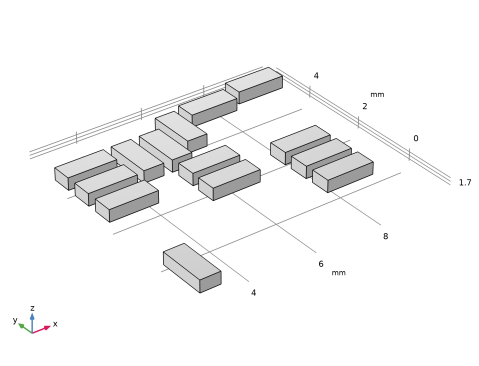
Here you can select the components to import from the PCB file. While these components do not affect the interpolation function, their outline will be extruded to generate domains that can become useful for setting up a simulation, for example when defining heat sources. After the add-in finishes, you could also create component domains manually using the geometry functionality or import from other sources.
16
From the 3D components list, choose Selected. In the table, select the Import checkboxes for R39, R48-R51, R78, R81, R87-R93.
17
Click Run button in the window toolbar to create material data.
While the add-in is running, the progress window is displayed. The top progress bar shows the total progress of the add-in, while bottom bar shows the progress for the current step that the add-in is working on, for example Processing layer: F.Cu.
Component 1 (comp1)
1
In the Model Builder window, click Component 1 (comp1).
2
Click the  Wireframe Rendering button in the Graphics toolbar.
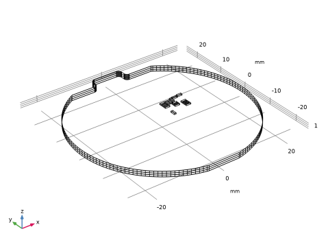
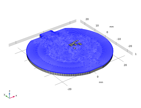
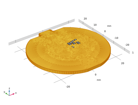
The simplified PCB geometry does not contain any copper traces and vias, as these are instead captured by the interpolation data with the material properties.
3
Click the  Wireframe Rendering button in the Graphics toolbar.
Geometry 1
Import 1 (imp1)
The geometry sequence generated by the add-in includes the operations for creating the simplified representation of the components and the PCB where the board’s outline, thickness and layer distribution are preserved.
1
In the Model Builder window, expand the Component 1 (comp1) > Geometry 1 node, then click Import 1 (imp1).
2
In the Settings window for Import, click  Build Selected.
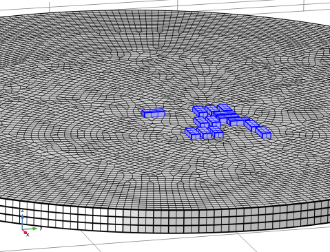
The first import node is set up to generate the components. The outlines are read from the file and extruded to create the component domains.
Extract 1 (extract1)
1
In the Model Builder window, click Extract 1 (extract1).
2
In the Settings window for Extract, click  Build Selected.
Since the import generates domains for all components, the Extract 1 feature is used to retain only those selected earlier.
3
Click the  Zoom Extents button in the Graphics toolbar.
Import 2 (imp2)
1
In the Model Builder window, click Import 2 (imp2).
2
In the Settings window for Import, click  Build Selected.
This second import node is configured to import one dielectric layer with the thickness set to zero. The resulting face is used at the next step to extrude the board geometry.
3
Click the  Zoom Extents button in the Graphics toolbar.
Extrude 1 (ext1)
1
In the Model Builder window, click Extrude 1 (ext1).
2
In the Settings window for Extrude, click  Build Selected.
The distances specified in the Distances table for Extrude 1 correspond to the layer elevations in the PCB file. Thus, in the resulting object the separate domains represent the layers from the PCB file.
Box Selection 1 (boxsel1)
1
In the Model Builder window, click Box Selection 1 (boxsel1).
2
In the Settings window for Box Selection, click  Build Selected.
This coordinate-based selection has been added for selecting the topmost boundary of the board which is used in the meshing sequence.
Interpolation 1
The add-in generates a space-dependent interpolation functions that mathematically models the effect of the board’s traces and vias allowing for the substitution of detailed geometry with equivalent material property fields.
1
In the Model Builder window, expand the Component 1 (comp1)>Definitions node, then click Interpolation 1.
The functions that define the material properties are listed in the Functions table.
Materials
Material 3 (mat3)
1
In the Model Builder window, expand Component 1 (comp1)>Materials node, then click Material 3 (mat3).
2
In the Settings window for Material, locate the Material Contents section.
For each material property defined in the table, the Value column contains the corresponding interpolation function.
Add Material
While the add-in has configured the material properties of the board, it remains to choose an appropriate material for the imported resistors.
1
In the Home toolbar, click  Add Material to open the Add Material window.
2
Go to the Add Material window.
3
In the tree, select Built-in > Alumina.
4
Click the Add to Component button in the window toolbar.
5
In the Home toolbar, click  Add Material to close the Add Material window.
Materials
Alumina (mat4)
1
In the Settings window for Material, locate the Geometric Entity Selection section.
2
From the Selection list, choose Extract 1.
Heat Transfer in Solids (ht)
Heat Source 1
1
In the Physics toolbar, click  Domains and choose Heat Source.
2
In the Settings window for Heat Source, locate the Domain Selection section.
3
From the Selection list, choose Extract 1.
4
Locate the Heat Source section. From the Heat source list, choose Heat rate.
5
In the P0 text field, type 14*0.0625[W].
Heat Flux 1
1
In the Physics toolbar, click  Boundaries and choose Heat Flux.
To more easily select the boundaries subjected to natural convection, create a selection in the geometry that encompasses all exterior boundaries of the board and components.
Geometry 1
Form Union (fin)
1
In the Model Builder window, under Component 1 (comp1) > Geometry 1 click Form Union (fin).
2
In the Settings window for Form Union/Assembly, click  Build Selected.
By first building the Form union node, you ensure that the Adjacent Selection feature added in the next step is inserted after Form Union. This is important to avoid selecting boundaries that are between the components and the board.
Exterior boundaries
1
In the Geometry toolbar, click  Selections and choose Adjacent Selection.
2
In the Settings window for Adjacent Selection, type Exterior boundaries in the Label text field.
3
Locate the Input Entities section. Click  Add.
4
In the Add dialog, in the Input selections list, choose Extract 1 and Extrude 1.
5
Heat Transfer in Solids (ht)
Heat Flux 1
1
In the Model Builder window, under Component 1 (comp1) > Heat Transfer in Solids (ht) click Heat Flux 1.
2
In the Settings window for Heat Flux, locate the Boundary Selection section.
3
From the Selection list, choose Exterior boundaries.
4
Locate the Heat Flux section. From the Flux type list, choose Convective heat flux.
5
In the h text field, type 5[W/(m^2*K)].
6
In the Text text field, type 20[degC].
Solid Mechanics (solid)
In the Model Builder window, under Component 1 (comp1) click Solid Mechanics (solid).
Rigid Motion Suppression 1
1
In the Physics toolbar, click  Domains and choose Rigid Motion Suppression.
2
In the Settings window for Rigid Motion Suppression, locate the Contributing Points section.
3
From the list, choose From selection input.
4
Locate the Point Selection section. From the Selection list, choose Extrude 1.
Multiphysics
Thermal Expansion 1 (te1)
1
In the Model Builder window, under Component 1 (comp1) > Multiphysics click Thermal Expansion 1 (te1).
2
In the Settings window for Thermal Expansion, locate the Model Input section.
3
From the Tref list, choose User defined. In the associated text field, type 20[degC].
Mesh 1
Free Quad 1
In the Model Builder window, expand the Mesh 1 node.
Size 1
1
In the Model Builder window, expand the Free Quad 1 node.
2
Right-click Size 1 and choose Build Selected.
The add-in created a mesh that takes into account the 3D grid used for generating the interpolation data. Specifically, the maximum element size is configured to be five times the interpolation grid size, and the minimum element size is set to equal the grid size. You can adjust these parameters to perform a mesh sensitivity study and determine an optimal resolution for your analysis. However, it is important to note that meshing with element size finer than the underlying interpolation grid will not yield further gains in solution accuracy.
Swept 1
1
In the Model Builder window, expand the Component 1 (comp1) > Mesh 1 > Swept 1 node.
2
Right-click Swept 1 and choose Build Selected.
Notice that the Swept 1 operation applied one element layer per domain. The number of elements in the sweep direction can be changed in the Distribution 1 attribute to Swept 1.
Next, generate a mesh for the resistor domains that are not meshed by the add-in.
Swept 2
1
In the Mesh toolbar, click  Swept.
2
In the Settings window for Swept, click  Build Selected.
Study 1
Step 1: Stationary
In the Home toolbar, click  Compute.
Result Templates
To visualize the temperature distribution inside the PCB, create a multislice plot.
1
In the Results toolbar, click  Result Templates to open the Result Templates window.
2
Go to the Result Templates window.
3
In the tree, select Study 1/Solution 1 (sol1) > Solid Mechanics > Displacement (solid) and Study 1/Solution 1 (sol1) > Heat Transfer in Solids > Temperature, Multislice (ht).
4
Click the Add Result Template button in the window toolbar.
5
In the Results toolbar, click  Result Templates to close the Result Templates window.
Results
Multislice 1
1
In the Model Builder window, expand the Temperature, Multislice (ht) node, then click Multislice 1.
2
In the Settings window for Multislice, locate the Expression section.
3
From the Unit list, choose °C.
4
Locate the Multiplane Data section. Find the X-planes subsection. From the Entry method list, choose Coordinates.
5
In the Coordinates text field, type 6.35[mm].
6
Find the Y-planes subsection. From the Entry method list, choose Coordinates.
7
In the Coordinates text field, type 4.4[mm].
8
Find the Z-planes subsection. From the Entry method list, choose Coordinates.
9
In the Coordinates text field, type -0.0175[mm].
10
In the Temperature, Multislice (ht) toolbar, click  Plot.
Displacement (solid)
1
Click the  Go to Default View button in the Graphics toolbar.
2
In the Model Builder window, under Results click Displacement (solid).
Material Properties Plot
Finally, create a slice plot at an elevation that corresponds to one of the interior metal layers to visualize the spatial distribution of a material property obtained by evaluating the interpolation function.
1
In the Results toolbar, click  3D Plot Group.
2
In the Settings window for 3D Plot Group, type Material Properties Plot in the Label text field.
Slice 1
1
Right-click Material Properties Plot and choose Slice.
2
In the Settings window for Slice, locate the Expression section.
3
In the Expression text field, type ht.Cp.
4
Locate the Plane Data section. From the Plane list, choose XY-planes.
5
From the Entry method list, choose Coordinates.
6
In the Z-coordinates text field, type 1[mm].
7
Locate the Coloring and Style section. From the Color table list, choose Traffic.
8
From the Color table transformation list, choose Reverse.
9
In the Material Properties Plot toolbar, click  Plot.
10
Click the  Go to XY View button in the Graphics toolbar.
To compare the displayed plot to the detailed geometry of the traces at the corresponding elevation, see Figure 1.