|
|
1
|
|
2
|
Click
|
|
1
|
|
2
|
|
3
|
Click
|
|
4
|
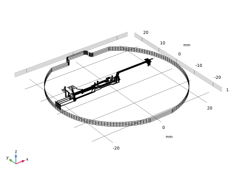
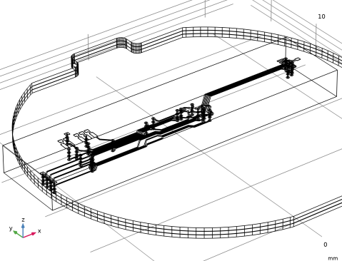
Browse to the model’s Application Libraries folder and double-click the file audioStreamingPCB.xml.
|
|
5
|
|
6
|
|
7
|
In the table, select the checkbox for DRILL:F.CU_B.CU to also import this layer.
|
|
8
|
|
9
|
In the text field, type bt_p.
|
|
10
|
Click
|
|
11
|
In the text field, type wl_s.
|
|
12
|
Click
|
|
13
|
|
14
|
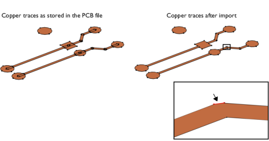
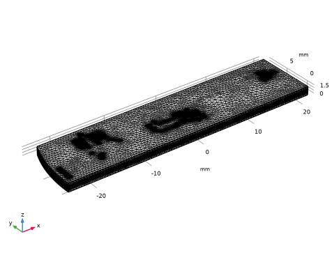
Select the Eliminate short edges checkbox.
|
|
15
|
Find the Ignore vertices in layers subsection. In the Maximum edge length text field, type 0.017[mm].
|
|
16
|
|
17
|
|
1
|
|
2
|
|
3
|
|
4
|
|
5
|
|
6
|
|
7
|
|
8
|
|
9
|
|
10
|
|
11
|
|
12
|
Locate the Selections of Resulting Entities section. Select the Resulting objects selection checkbox.
|
|
13
|
|
14
|
|
1
|
|
2
|
|
3
|
|
4
|
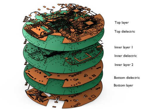
In the Set formula text field, type (imp1.B_CU + imp1.IN1_CU+imp1.IN2_CU+imp1.F_CU+imp1.DIELECTRIC_1+imp1.DIELECTRIC_2+imp1.DIELECTRIC_3)*blk1.
|
|
5
|
Click
|
|
1
|
|
2
|
|
1
|
|
2
|
|
3
|
|
4
|