|
|
1
|
|
2
|
Click
|
|
1
|
|
2
|
|
3
|
Click
|
|
4
|
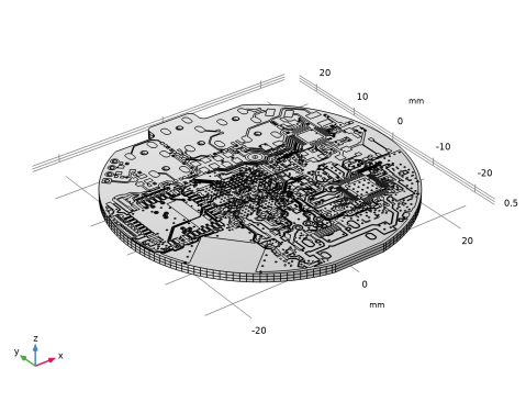
Browse to the model’s Application Libraries folder and double-click the file audioStreamingPCB.xml.
|
|
5
|
|
7
|
|
8
|
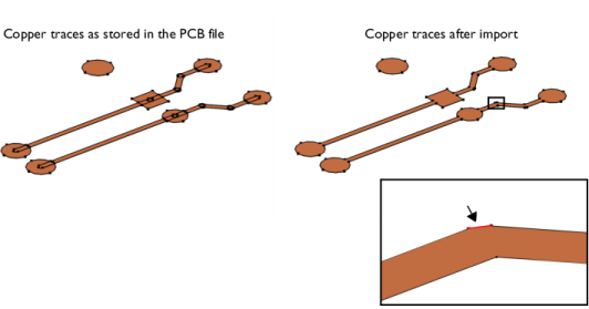
Clear the Create domains for the cores of plated holes checkbox.
|
|
9
|
Select the Via cores through metal layers checkbox.
|
|
10
|
|
1
|
|
2
|
|
1
|
|
2
|
|
3
|
|
1
|
|
2
|
|
3
|
|
4
|
|
5
|
Click
|
|
6
|
|
7
|
|
8
|
|
1
|
|
2
|
|
3
|
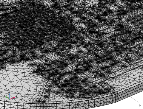
Select the Automatic detection of small details checkbox.
|
|
4
|
|
5
|
In the Geometry Cleanup dialog that opens, click Clean up Automatically to automatically clean up the geometry.
|
|
1
|
|
2
|
Go to the Add Material window.
|
|
3
|
|
4
|
Click the Add to Component button in the window toolbar.
|
|
1
|
|
2
|
|
1
|
Go to the Add Material window.
|
|
2
|
|
3
|
Click the Add to Component button in the window toolbar.
|
|
4
|
|
1
|
|
2
|
|
3
|
|
4
|
|
1
|
|
2
|
|
3
|
|
4
|