|
|
1
|
|
2
|
Click
|
|
1
|
|
2
|
|
3
|
Click
|
|
4
|
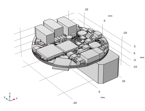
Browse to the model’s Application Libraries folder and double-click the file audioStreamingPCB.xml.
|
|
6
|
Click to expand the Pads section. In the table, enter the following settings:
|
|
7
|
Click to expand the Drill Holes section. Here you can enter the plating thickness for plated holes and vias in the board. The core via domains will be surrounded with copper domains of this thickness. This setting has no effect on non-plated drill holes in the file.
|
|
8
|
|
9
|
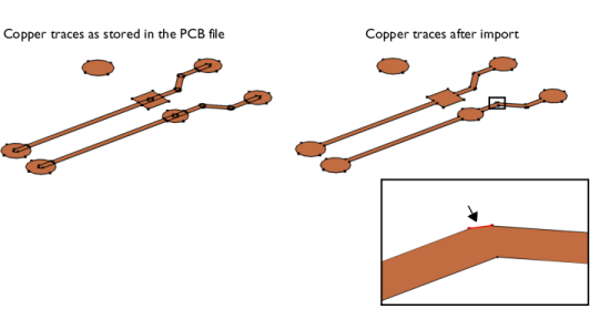
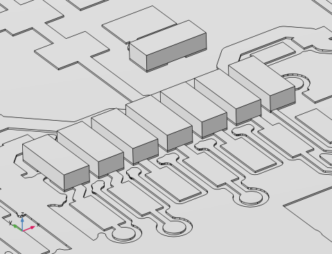
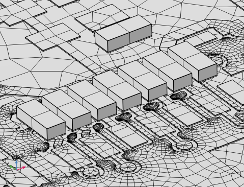
Click to expand the Simplify and Repair section. Using the tools in this section is important when extruding the copper layers during the import. Since the small geometric details are eliminated before the layers are extruded, this method can be more robust when compared to defeaturing the final geometry.
|
|
10
|
Select the Eliminate short edges checkbox.
|
|
11
|
Find the Ignore vertices in layers subsection. In the Maximum edge length text field, type 0.0032[mm].
|
|
12
|
|
1
|
|
2
|
Go to the Selection List window.
|
|
3
|
|
4
|
|
5
|
|
1
|
|
2
|
|
3
|
Click
|
|
4
|
Browse to the model’s Application Libraries folder and double-click the file audioStreamingPCB.xml.
|
|
5
|
|
6
|
|
7
|
|
1
|
|
2
|
|
3
|
|
1
|
|
2
|
|
3
|
|
4
|
Click
|
|
1
|
|
2
|
|
3
|
|
4
|
|
5
|
|
6
|
|
1
|
|
2
|
|
3
|
|
4
|
Click
|
|
1
|
|
2
|
|
3
|
|
4
|