PDF

Optical Ring Resonator Notch Filter 3D
Introduction
The simplest optical ring resonator consists of a straight waveguide and a ring waveguide. The two waveguide cores are placed close to each other, so light couples from one waveguide to the other.
When the length of the ring waveguide is an integer number of wavelengths, the ring waveguide is resonant to the wavelength and the light power stored in the ring builds up.
The wave transmitted through the straight waveguide is the interference of the incident wave and the wave that couples over from the ring to the straight waveguide.
Schematically, you can think of the ring resonator as shown in Figure 1. A part of the incident wave Ei1 is transmitted in the straight waveguide, whereas a fraction of that field couples over to the ring. Similarly, some of the light in the ring couples over to the straight waveguide, whereas the rest of that wave continues around the ring waveguide.
Figure 1: Schematic of an optical ring resonator, showing the incident fields Ei1 and Ei2 and the transmitted/coupled fields Et1 and Et2. The transmission and coupling coefficients t and κ are also indicated, as well as the round-trip loss L.
The transmitted fields are related to the incident fields through the matrix-vector relation
(1).
The matrix elements defined above assure that the total input power equals the total output power,
(2),
by assuming that the transmission and coupling coefficients are related by
(3).
Furthermore, as the wave propagates around the ring waveguide, one gets the relation
(4),
where L is the loss coefficient for the propagation around the ring and is the accumulated phase.
Combining Equation 1, Equation 3, and Equation 4, the transmitted field can be written
(5).
Here the transmission coefficient is separated into the transmission loss |t| and the corresponding phase ,
(6).
Notice that on resonance, when is an integer multiple of 2π, and when |t| = L, the transmitted field is zero. The condition |t| = L is called critical coupling. Thus, when the coupler transmission loss balances the loss for the wave propagating around the ring waveguide, one gets the optimum condition for a bandstop filter, a notch filter.
The procedure to optimize the filter is as follows:
1
Calculate the transmittance |t|2 for some values of the distance between the straight and the ring waveguide. Here, your should just include half (or a part) of the ring.
2
Calculate the loss coefficient L for some values of the ring radius. In this case, define a geometry with a short piece of straight waveguide, followed by half of the ring, and, finally, another short piece of straight waveguide. The short pieces of straight waveguide help to launch and properly absorb the propagating wave.
3
4
5
However, before starting a full 3D design, it is often good to begin with a 2D model, as described in the Optical Ring Resonator Notch Filter model.
Model Definition
This application is set up using the Electromagnetic Waves, Beam Envelopes interface, to handle the propagation over distances that are many wavelengths long. Since the wave propagates in essentially one direction along the straight waveguide and along the waveguide ring, the unidirectional formulation is used. This assumes that the electric field for the wave can be written as
(7),
where E1 is a slowly varying field envelope function and is an approximation of the propagation phase for the wave. The definitions used for the phase in the straight and ring waveguide are shown in Table 1, Table 2, and Table 3.
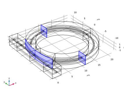
The parameters r0 and dx correspond, respectively, to the curvature radius of the ring waveguide and to the separation between the straight and ring waveguide cores. The phase approximation defined in the tables above is discontinuous at the boundary between the straight waveguide and the ring waveguide as well as at the boundary between the left and the right ring waveguide domains. To handle this phase discontinuity and thereby the discontinuity in the field envelope, E1, a Field Continuity boundary condition is used at the aforementioned boundaries. The Field Continuity boundary condition ensures that the tangential components of the electric and the magnetic fields are continuous at the boundary, despite the phase jump.
In this model, not only the guided wave needs to be resolved. There is also coupling to radiating modes that needs to be resolved. Thus, the mesh needs resolve the beating between these different waves. Instead of making a very fine mesh, cubic shape orders are used when solving for the electric field. However, when running this model on a Windows PC, approximately 24 GB of RAM is required.
Results and Discussion
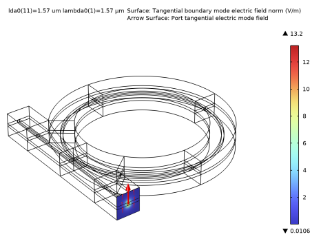
Figure 2 shows the mode field at the launch port. As the height of the waveguide core is slightly larger than the width of the core, the lowest order mode is polarized in the z direction.
Figure 2: The mode field norm and polarization at the launch port.
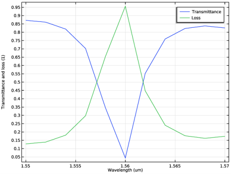
Figure 3 shows that the transmittance at the resonance wavelength, 1.56 mm, is very small (below 5%), as the device was designed to approximately match the transmittance through the coupler with the loss coefficient in the ring (see the discussion in the Introduction).
Figure 3: The transmittance and loss spectra.
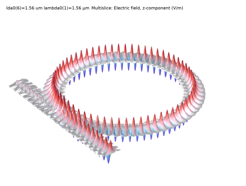
Figure 4 shows the z-component of the electric field at the resonance wavelength. Notice that the field in the straight waveguide is very weak after the coupler region, due to the destructive interference between the light passing straight through the coupler region and the light coupled back in from the ring. Furthermore, it is clear that there is a noticeable loss when the wave propagates around the ring.
Figure 4: The z-component of the electric field at the resonance wavelength 1.56 μm.
Notes About the COMSOL Implementation
This model geometry is easily set up by importing a geometry part from the COMSOL Part Libraries. The rectangular waveguide coupling between a straight and a ring waveguide section, with the core embedded in a cladding domain, is available in the Wave Optics Module Part Library under Rectangular Waveguides.
Predefined geometry parts can be quickly modified by changing the default input parameters. Moreover, geometry parts provide targeted selections of domains and boundaries that greatly simplify the model building. As demonstrated in this model, these built-in selections are useful when adding materials, physics features and mesh sequences.
Application Library path: Wave_Optics_Module/Waveguides_and_Couplers/optical_ring_resonator_3d
Modeling Instructions
From the File menu, choose New.
New
In the New window, click  Model Wizard.
Model Wizard
1
In the Model Wizard window, click  3D.
2
In the Select Physics tree, select Optics>Wave Optics>Electromagnetic Waves, Beam Envelopes (ewbe).
3
Click Add.
4
Click  Study.
5
In the Select Study tree, select Preset Studies for Selected Physics Interfaces>Wavelength Domain.
6
Global Definitions
Parameters 1
1
In the Model Builder window, under Global Definitions click Parameters 1.
2
In the Settings window for Parameters, locate the Parameters section.
3
Click  Load from File.
4
Geometry 1
1
In the Model Builder window, under Component 1 (comp1) click Geometry 1.
2
In the Settings window for Geometry, locate the Units section.
3
From the Length unit list, choose µm.
Part Libraries
1
In the Home toolbar, click  Windows and choose Part Libraries.
2
In the Part Libraries window, select Wave Optics Module>Rectangular Waveguides>rectangular_waveguide_straight_to_ring_coupler in the tree.
3
Click  Add to Geometry.
Geometry 1
Rectangular Waveguide Straight-to-Ring Coupler 1 (pi1)
1
In the Model Builder window, under Component 1 (comp1)>Geometry 1 click Rectangular Waveguide Straight-to-Ring Coupler 1 (pi1).
2
In the Settings window for Part Instance, locate the Input Parameters section.
3
4
Locate the Position and Orientation of Output section. Find the Displacement subsection. In the yw text field, type -r0-w_clad/2.
5
Click to expand the Domain Selections section. Click the  Wireframe Rendering button in the Graphics toolbar, to make it easier to see the selections.
6
7
Click to expand the Boundary Selections section. In the table, enter the following settings:
8
Click  Build All Objects.
Definitions
First add a few selections that will be useful when defining the mesh.
Core Boundaries
1
In the Definitions toolbar, click  Adjacent.
2
In the Settings window for Adjacent, type Core Boundaries in the Label text field.
3
Locate the Input Entities section. Under Input selections, click  Add.
4
In the Add dialog box, select Core (Rectangular Waveguide Straight-to-Ring Coupler 1) in the Input selections list.
5
6
In the Settings window for Adjacent, locate the Output Entities section.
7
Select the Interior boundaries check box.
Triangular Mesh Core Boundaries
1
In the Definitions toolbar, click  Intersection.
2
In the Settings window for Intersection, type Triangular Mesh Core Boundaries in the Label text field.
3
Locate the Geometric Entity Level section. From the Level list, choose Boundary.
4
Locate the Input Entities section. Under Selections to intersect, click  Add.
5
In the Add dialog box, in the Selections to intersect list, choose Core Boundaries and Triangular mesh (Rectangular Waveguide Straight-to-Ring Coupler 1).
6
Materials
Cladding
1
In the Model Builder window, under Component 1 (comp1) right-click Materials and choose Blank Material.
2
In the Settings window for Material, type Cladding in the Label text field.
3
Locate the Material Contents section. In the table, enter the following settings:
Core
1
Right-click Materials and choose Blank Material.
2
In the Settings window for Material, type Core in the Label text field.
3
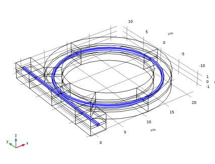
Locate the Geometric Entity Selection section. From the Selection list, choose Core (Rectangular Waveguide Straight-to-Ring Coupler 1).
4
Locate the Material Contents section. In the table, enter the following settings:
Definitions
Before setting up the physics, first add the definition of the phase variable that will be used by the Electromagnetic Waves, Beam Envelopes interface.
Variables 1
1
In the Model Builder window, under Component 1 (comp1) right-click Definitions and choose Variables.
2
In the Settings window for Variables, locate the Geometric Entity Selection section.
3
From the Geometric entity level list, choose Domain.
4
From the Selection list, choose Straight domain (Rectangular Waveguide Straight-to-Ring Coupler 1).
5
Locate the Variables section. In the table, enter the following settings:
Here, ewbe.beta_1 is the propagation constant for the first port. This port will be defined when the physics is set up in the next steps. As the variable not yet exists, COMSOL warns about this condition by displaying the expression in orange.
Variables 2
1
Right-click Variables 1 and choose Duplicate.
2
In the Settings window for Variables, locate the Geometric Entity Selection section.
3
From the Selection list, choose Ring domain 1 (Rectangular Waveguide Straight-to-Ring Coupler 1).
4
Locate the Variables section. In the table, enter the following settings:
Variables 3
1
Right-click Variables 2 and choose Duplicate.
2
In the Settings window for Variables, locate the Geometric Entity Selection section.
3
From the Selection list, choose Ring domain 2 (Rectangular Waveguide Straight-to-Ring Coupler 1).
4
Locate the Variables section. In the table, enter the following settings:
Electromagnetic Waves, Beam Envelopes (ewbe)
Now, use the phase variables when configuring the physics interface.
1
In the Model Builder window, under Component 1 (comp1) click Electromagnetic Waves, Beam Envelopes (ewbe).
2
In the Settings window for Electromagnetic Waves, Beam Envelopes, locate the Wave Vectors section.
3
From the Number of directions list, choose Unidirectional.
4
From the Type of phase specification list, choose User defined.
5
In the φ1 text field, type phi.
6
Click to expand the Discretization section. From the Electric field envelopes list, choose Cubic, to improve the spatial resolution.
Port 1
1
In the Physics toolbar, click  Boundaries and choose Port.
2
In the Settings window for Port, locate the Boundary Selection section.
3
From the Selection list, choose Port 1 (Rectangular Waveguide Straight-to-Ring Coupler 1).
4
Locate the Port Properties section. From the Type of port list, choose Numeric.
Port 2
1
In the Physics toolbar, click  Boundaries and choose Port.
2
In the Settings window for Port, locate the Boundary Selection section.
3
From the Selection list, choose Port 2 (Rectangular Waveguide Straight-to-Ring Coupler 1).
4
Locate the Port Properties section. From the Type of port list, choose Numeric.
Scattering Boundary Condition 1
1
In the Physics toolbar, click  Boundaries and choose Scattering Boundary Condition.
2
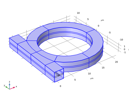
In the Settings window for Scattering Boundary Condition, locate the Boundary Selection section.
3
From the Selection list, choose Transverse perimeter (Rectangular Waveguide Straight-to-Ring Coupler 1).
4
Click the  Show More Options button in the Model Builder toolbar.
5
In the Show More Options dialog box, select Physics>Advanced Physics Options in the tree.
6
In the tree, select the check box for the node Physics>Advanced Physics Options.
7
Field Continuity 1
1
In the Physics toolbar, click  Boundaries and choose Field Continuity.
2
In the Settings window for Field Continuity, locate the Boundary Selection section.
3
From the Selection list, choose Field continuity (Rectangular Waveguide Straight-to-Ring Coupler 1).
Mesh 1
Now, define the mesh. As in addition to the guided wave there is a fair amount of radiation loss in this model, the mesh must be rather fine.
Free Triangular 1
1
In the Mesh toolbar, click  Boundary and choose Free Triangular.
2
In the Settings window for Free Triangular, locate the Boundary Selection section.
3
From the Selection list, choose Triangular mesh (Rectangular Waveguide Straight-to-Ring Coupler 1).
Size
1
In the Model Builder window, click Size.
2
In the Settings window for Size, locate the Element Size section.
3
Click the Custom button.
4
Locate the Element Size Parameters section. In the Maximum element size text field, type w_clad/5.
5
In the Maximum element growth rate text field, type 2, to slightly reduce the number of mesh elements.
Size 1
1
In the Model Builder window, right-click Free Triangular 1 and choose Size.
2
In the Settings window for Size, locate the Geometric Entity Selection section.
3
From the Selection list, choose Triangular Mesh Core Boundaries.
4
Locate the Element Size section. Click the Custom button.
5
Locate the Element Size Parameters section.
6
Select the Maximum element size check box. In the associated text field, type w_core/2.
Swept 1
1
In the Mesh toolbar, click  Swept.
2
In the Settings window for Swept, locate the Domain Selection section.
3
From the Geometric entity level list, choose Domain.
4
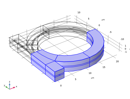
From the Selection list, choose Mesh source domain (Rectangular Waveguide Straight-to-Ring Coupler 1).
Size 1
1
Right-click Swept 1 and choose Size.
2
In the Settings window for Size, locate the Element Size section.
3
Click the Custom button.
4
Locate the Element Size Parameters section.
5
Select the Maximum element size check box. In the associated text field, type wl0/2.
Copy Domain 1
1
In the Model Builder window, right-click Mesh 1 and choose Copying Operations>Copy Domain.
2
In the Settings window for Copy Domain, locate the Source Domains section.
3
From the Selection list, choose Mesh source domain (Rectangular Waveguide Straight-to-Ring Coupler 1).
4
Locate the Destination Domains section. From the Selection list, choose Mesh destination domain (Rectangular Waveguide Straight-to-Ring Coupler 1).
5
Click  Build All.
Study 1
Boundary Mode Analysis
1
In the Study toolbar, click  Study Steps and choose Other>Boundary Mode Analysis.
2
In the Settings window for Boundary Mode Analysis, locate the Study Settings section.
3
In the Mode analysis frequency text field, type f0.
4
In the Search for modes around text field, type n_core.
Step 3: Boundary Mode Analysis 1
1
Right-click Study 1>Step 2: Boundary Mode Analysis and choose Duplicate.
2
In the Settings window for Boundary Mode Analysis, locate the Study Settings section.
3
In the Port name text field, type 2.
Step 1: Wavelength Domain
1
In the Model Builder window, click Step 1: Wavelength Domain.
2
In the Settings window for Wavelength Domain, locate the Study Settings section.
3
In the Wavelengths text field, type lda0.
4
Right-click Study 1>Step 1: Wavelength Domain and choose Move Down. Repeat this command once, to move the Wavelength Domain study step to the last position in the study sequence.
Parametric Sweep
1
In the Study toolbar, click  Parametric Sweep.
2
In the Settings window for Parametric Sweep, locate the Study Settings section.
3
4
5
In the Study toolbar, click  Compute.
Results
Electric Field (ewbe)
1
In the Settings window for 3D Plot Group, locate the Data section.
2
From the Parameter value (lda0 (um)) list, choose 1.56, to select the resonance wavelength.
Now, make a few adjustments to the plot to get a more detailed view of the result.
3
Locate the Plot Settings section. Clear the Plot dataset edges check box.
4
Click the  Show Legends button in the Graphics toolbar.
5
Click the  Show Grid button in the Graphics toolbar.
6
Click the  Show Axis Orientation button in the Graphics toolbar.
Electric Field
1
In the Model Builder window, expand the Electric Field (ewbe) node, then click Electric Field.
2
In the Settings window for Multislice, locate the Expression section.
3
In the Expression text field, type ewbe.Ez.
4
Locate the Multiplane Data section. Find the X-planes subsection. In the Planes text field, type 0.
5
Find the Y-planes subsection. In the Planes text field, type 0.
6
Locate the Coloring and Style section. Click  Change Color Table.
7
In the Color Table dialog box, select Wave>WaveLight in the tree.
8
Deformation 1
1
Right-click Electric Field and choose Deformation.
2
In the Settings window for Deformation, locate the Expression section.
3
In the Z-component text field, type ewbe.Ez.
4
Locate the Scale section.
5
Select the Scale factor check box. In the associated text field, type 5E-8.
Electric Field
1
In the Model Builder window, click Electric Field.
2
In the Settings window for Multislice, click to expand the Quality section.
3
From the Resolution list, choose Extra fine.
4
Click the  Zoom Extents button in the Graphics toolbar.
5
In the Electric Field (ewbe) toolbar, click  Plot.
At resonance, the waves in the straight waveguide and in the ring waveguide interfere to almost completely cancel out.
Transmittance and Loss (ewbe)
1
In the Model Builder window, under Results click Reflectance, Transmittance, and Absorptance (ewbe).
2
In the Settings window for 1D Plot Group, type Transmittance and Loss (ewbe) in the Label text field.
3
Locate the Plot Settings section. In the y-axis label text field, type Transmittance and loss (1).
Global 1
1
In the Model Builder window, expand the Transmittance and Loss (ewbe) node, then click Global 1.
2
In the Settings window for Global, locate the y-Axis Data section.
3
4
Click  Delete.
5
Click to expand the Legends section. From the Legends list, choose Manual.
6
7
In the Transmittance and Loss (ewbe) toolbar, click  Plot.
It is clear that at the resonance wavelength the transmission is very small (below 5 %), making the device behave as a notch filter.
Arrow Surface 1
1
In the Model Builder window, right-click Electric Mode Field, Port 1 (ewbe) and choose Arrow Surface.
2
In the Settings window for Arrow Surface, click Replace Expression in the upper-right corner of the Expression section. From the menu, choose Component 1 (comp1)>Electromagnetic Waves, Beam Envelopes>Ports>ewbe.tEmodex_1,...,ewbe.tEmodez_1 - Port tangential electric mode field.
3
In the Electric Mode Field, Port 1 (ewbe) toolbar, click  Plot.
The mode field is localized in and around the core, with a polarization in the z-direction.
Arrow Surface 1
1
In the Model Builder window, right-click Electric Mode Field, Port 2 (ewbe) and choose Arrow Surface.
2
In the Settings window for Arrow Surface, click Replace Expression in the upper-right corner of the Expression section. From the menu, choose Component 1 (comp1)>Electromagnetic Waves, Beam Envelopes>Ports>ewbe.tEmodex_2,...,ewbe.tEmodez_2 - Port tangential electric mode field.
3
In the Electric Mode Field, Port 2 (ewbe) toolbar, click  Plot.
As expected, the mode field for the second port is also polarized in the z-direction.