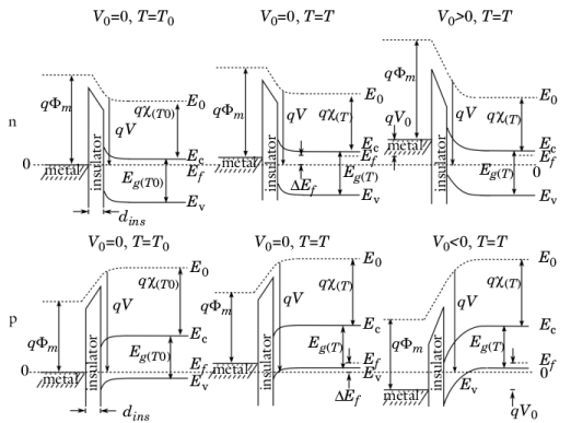
The band diagram for a thin insulating gate is shown in Figure 3-15. As for the ohmic contact, a change in the temperature of the device away from the equilibrium reference results in a shift of the metal and semiconductor Fermi levels (
ΔEf) on the absolute energy scale, given by
Equation 3-135. An applied potential further shifts the metal Fermi level with respect to the semiconductor Fermi level (which can be defined in regions away from the contact where little current flows).
When the Thin Insulator Gate boundary condition is used, the thin insulating layer is not included in the COMSOL Multiphysics model but its effect is included in the formulation of the boundary condition. The insulator is assumed to be so thin that the electric field (which must be perpendicular to the metal surface) is to a good approximation also perpendicular to the insulator-semiconductor boundary. When this is the case, the normal electric displacement field (
D) at the insulator-semiconductor interface can be written as:
where Vg is the potential on the gate,
V is the potential at the insulator-semiconductor interface,
dins is the thickness of the insulator,
εins is the relative dielectric permittivity of the insulator,
ε0 is the permittivity of free space, and
n is the outward normal of the semiconductor domain. From
Figure 3-15, the gate voltage with applied potential
V0 is given by:
where Φm is the metal work function.
ΔE
f is given by
Equation 3-135. Therefore:
When traps are present on the gate the traps accumulate charge as described in the Traps section. As a result of the charge on the boundary the electric displacement field is discontinuous across the interface and consequently:
where Q is the surface charge density due to the traps, given by
Equation 3-89 or
Equation 3-90. Consequently the form of
Equation 3-141 is modified so that: