You are viewing the documentation for an older COMSOL version. The latest version is
available here.
The Metal Contact boundary condition is used for modeling different types of metal-semiconductor junctions. The
Ideal Ohmic and
Ideal Schottky types of contact can be modeled with this feature. An optional infinitesimally thin resistive layer can be added using the
Contact resistance check box.
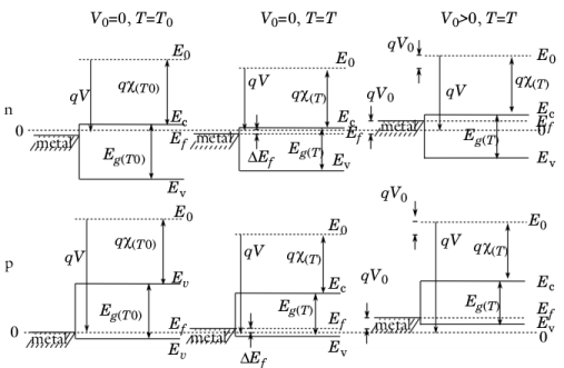
The ohmic contact option assumes local thermodynamic equilibrium at the contact. Note that in practice it is often used in nonequilibrium situations where the boundary condition imposed is no longer physical (for example in a forward biased p-n junction), which is reasonable provided that the junction is located some distance from the region of interest. Since equilibrium is assumed, both the hole and electron quasi-Fermi levels are equal at the boundary. Charge neutrality at the boundary is also assumed so there is no band bending and the band diagram takes the form shown in
Figure 3-12.
Since equilibrium is assumed, Equation 3-49 is used for the carrier concentrations but it is useful to write it in the alternative forms:
(3-130)

where Equation 3-77 is used to derive the expressions for
n and
p in terms of the effective intrinsic carrier concentration. The charge neutrality condition states:
(3-131)

Solve Equation 3-130 and
Equation 3-131 in a form convenient for numerical analysis by using the result
neqpeq=
γnγpni,eff2 (
Equation 3-93). Using this result with
Equation 3-131 gives:
peq must be positive therefore:
(3-132)

From Equation 3-130 the difference between the intrinsic level and the Fermi level can be determined in the following manner:
This result applies at arbitrary temperatures. Using Equation 3-93 and the above result, the conduction band energy level can be related to the intrinsic level and correspondingly to the equilibrium Fermi level in the following manner:
where the result Ev=Ec−Eg is used. The vacuum potential,
V, is therefore:
(3-133)

Equation 3-133 gives the vacuum potential relative to the Fermi level at an arbitrary temperature. However, it does not fix the vacuum potential on an absolute scale (the value of
Ef is not known on this scale). As discussed in
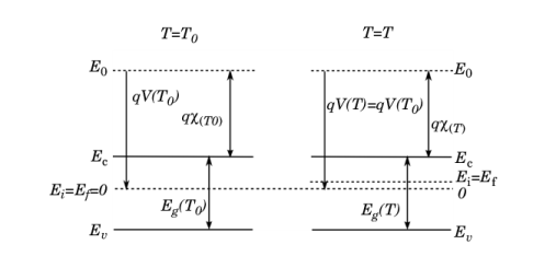
The Semiconductor Equations, COMSOL Multiphysics references the vacuum potential to the Fermi level in the equilibrium reference configuration (shown on the left of
Figure 3-12). Since the vacuum level adjusts to accommodate the space charge layers that are created in the device, it does not remain constant when the temperature is changed away from equilibrium. For an intrinsic semiconductor, however, the vacuum level remains constant when the temperature is changed. This is shown in
Figure 3-13.
Ef on the absolute scale must be set in a such a way that the limiting case of an intrinsic semiconductor is correct.
Using the above equation and Equation 3-133, and the fact that the intrinsic semiconductor has no band gap narrowing,
where χ0 is the electron affinity in the absence of band gap narrowing and
Eg0 is the energy gap in the absence of band gap narrowing. By definition
Ei(
T0)
= Ef(
T0)
= 0 therefore:
(3-134)

Equation 3-134 sets the value of the Fermi level relative to the zero in potential at temperature
T for an intrinsic semiconductor.
Ef(
T) is the offset in the energy scale relative to the equilibrium temperature for the particular case of an intrinsic semiconductor. Next consider a semiconductor with a nonuniform doping distribution but with a region of intrinsic semiconductor. The entire semiconductor is heated uniformly to raise its temperature from
T0 to
T1 (with no applied biases). The Fermi level in the intrinsic semiconductor changes according to
Equation 3-134. Since the whole sample is still at equilibrium, the Fermi level everywhere else in the sample must also change by the same amount.
Equation 3-134 gives the value of the Fermi level at equilibrium for any level of doping (in the absence of applied biases). The temperature-dependent (and doping-independent) offset is defined in the Fermi level:
(3-135)

Equation 3-133 can be written as:
So with an applied bias V0, the boundary condition on
V should be:
(3-136)

The ohmic contact boundary condition imposes Equation 3-132 on the carrier concentrations and
Equation 3-136 on the potential at the boundary. For the
Semiconductor Equilibrium study step, only the constraint on the electric potential is applied. Note that all metal contacts attached to the same
Semiconductor Material Model feature are biased at a common voltage, as dictated by the equilibrium condition. See
Semiconductor Equilibrium Study Settings on how to set the common bias voltage.
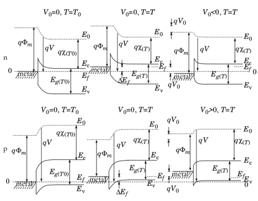
The ideal Schottky option adopts a simplified model for Schottky contacts, which is based largely on the approach introduced by Crowell and Sze (
Ref. 26). The semiconductor is assumed to be nondegenerate, since metal-degenerate semiconductor contacts are usually best represented by the Ideal Ohmic option.
Here, n is the outward normal of the semiconducting domain,
vn and
vp are the recombination velocities for holes and electrons, respectively, and
n0 and
p0 are the quasi-equilibrium carrier densities — that is, the carrier densities that would be obtained if it were possible to reach equilibrium at the contact without altering the local band structure.
n0 and
p0 are correspondingly defined as though the Fermi level of the semiconductor at the boundary is equal to that of the metal. From
Figure 3-14 n0 and
p0 are given by:
(3-137)

(3-138)

Here, Φm is the metal work function, E
fm is the metal Fermi level, and
ΦB is the emission barrier height for electrons (from the metal). The observed barrier heights of Schottky junctions frequently do not conform to
Equation 3-138, largely as a result of the complexities discussed previously. From a practical perspective, the value of
ΦB can be determined experimentally and, consequently, can be considered as an input into the model (COMSOL Multiphysics makes it possible to directly enter the barrier height or to compute the ideal barrier height from the material properties).
The recombination velocities vn and
vp are determined by assuming that the dominant source of current across the junction is thermionic emission.
Ref. 3 provides a full derivation of this case, which shows that, if thermionic emission is dominant:
(3-139)

Here, An* and
Ap* are the effective Richardson’s constants for electrons and holes, respectively (these are essentially material properties related to the thermionic emission —
Ref. 3 has details). The Schottky contact boundary condition allows the recombination velocities to be user defined or to be determined from
Equation 3-139. In addition, an extra current contribution can be specified with either a user-defined scaling factor or the scaling factor computed using the
WKB Tunneling Model.
Equation 3-137,
Equation 3-138, and
Equation 3-139 specify the boundary condition on the currents imposed at a Schottky contact. The boundary condition on the voltage can be determined from
Figure 3-14:
(3-140)

Equation 3-140 is used by COMSOL Multiphysics to constrain the potential at the boundary. For the
Semiconductor Equilibrium study step, only the constraint on the electric potential is applied. Note that all metal contacts attached to the same
Semiconductor Material Model feature are biased at a common voltage, as dictated by the equilibrium condition. See
Semiconductor Equilibrium Study Settings on how to set the common bias voltage.