You are viewing the documentation for an older COMSOL version. The latest version is
available here.
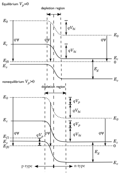
Most practical simulations deal with a band structure that varies in space — it is therefore necessary to define quantities such as the band energies with respect to a reference energy. In order to make the definition of boundary conditions simpler, the reference energy chosen is the Fermi energy in an equilibrium state when no potentials are applied to any of the boundaries in the system and when there are no thermal gradients in the system (note that in COMSOL Multiphysics, the reference temperature used to define the equilibrium Fermi energy can be changed in the Semiconductor interface’s Settings window under Reference Temperature). This is illustrated in
Figure 3-7 for an isothermal, abrupt
p-n junction (that is a boundary between a p- and n-doped region of a semiconductor with a constant doping level on the two sides of the device). In equilibrium the Fermi energy is well-defined and is constant throughout space (since there are no gradients in the Fermi level/chemical potential). As a result in the immediate vicinity of the junction, the bands bend to accommodate a constant Fermi energy. In this region of
band bending the Fermi level lies close to the center of the gap and consequently the carriers are depleted — this is known as the
depletion region. A space charge layer is associated with the depletion region since the charges of the ionized donors and acceptors are no longer compensated by free carriers. It is the space charge layer that generates an electric field and the corresponding potential gradient that results in the bending of the vacuum level,
E0, and the conduction band and valence band edges (
Ec and
Ev, respectively). This results in a self-consistent picture of the band structure in the vicinity of the junction. As a result of the bending of the vacuum level and bands, a built-in potential,
Vbi, develops across the junction. When an additional potential difference is applied to the p-side of the junction,
Vp, the junction is in a condition known as reverse bias. The Fermi energy is no longer well-defined in the vicinity of the depletion region, but the equilibrium Fermi level,
Ef0 is still used as a reference potential. Away from the depletion region the semiconductor is close to equilibrium and the concept of the Fermi level can still be applied. On the p-side of the junction, the Fermi energy shifts up to a value
Ef1, which differs from
Ef0 by
qVp where
q is the electron charge.
In the most general case the electron affinity, qχ = E0 − Ec, and the band gap,
Eg = Ec –Ev, can vary with position. However, the values can be considered to be material properties. This means that the conduction band edge cannot be parallel to the valence band edge or to the vacuum level (this is not shown in
Figure 3-7).
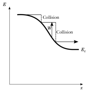
Consider the motion of an individual electron moving in the curved conduction band (see Figure 3-8). Between collisions, the energy of the electron remains approximately constant (although the force accelerates the electron, its velocity only increases slightly between collisions). The energy of the electron measured with respect to the band edge,
W, increases as a result of band bending. The total energy associated with an electron is given by:
As discussed in The Semiclassical Model, the evolution of the distribution function for electrons and holes is governed by the Boltzmann equation (see
Equation 3-40). Since this equation is difficult to solve, it is common to make simplifying approximations in its solution. Ultimately these approximations produce the drift-diffusion equations. The analysis presented here is based on
Ref. 12 and
Ref. 13.
Where f0 (
E,
Efn,
T) is the Fermi function for electrons and
f0h (
E,
Efp,
T) is the Fermi function for holes. This is essentially the simplest form of the collision term that returns the electrons to the Fermi-Dirac distribution desired. In practice this assumption is a significant simplification;
Ref. 1 and
Ref. 2 provide more detailed discussions of collision mechanisms in real solids.
For compactness, the explicit dependence of f0 and
τ is dropped. Considering first the electron density, the assumption that the
electron distribution function is close to its quasi-equilibrium state allows the distribution function to be written in the form:
where f1 <<
f0. The spatial gradient terms are dominated by terms involving the gradient of
f0, so the
f1 terms are neglected in comparison to these. Likewise the term
df/dt is also small since the deviation from the quasi-equilibrium is small and the
f0 term varies on time scales much slower than the collision time if the temperature is a function of time. The Boltzmann equation can be expressed in the approximate form:
(3-56)

Next the gradients in f0=1/(1+exp[(
E-
Efn)/(
kbT)]) are expressed in terms of parameters related to the band structure, using the chain rule:
(3-57)

(3-58)

Substituting Equation 3-58 and
Equation 3-57 into
Equation 3-56, using the definition
E = Ec + W and rearranging gives:
The final equality holds because f1 is an odd function when integrated over the region of k-space in the vicinity of a band edge and
f0 is an even function (assuming, without loss of generality, that the origin of k-space at the band minimum). To see why this is the case, consider
Equation 3-38 in
The Semiclassical Model (shown below for convenience).
In equilibrium (f = f0) no current flows so the integrand must be an odd function (since it is not zero over all k-space). Since the origin is at a band minimum,
∂E(k)/
∂k is odd so
f0 must be even. Deviations from equilibrium produce a current without changing the total number of electrons, so
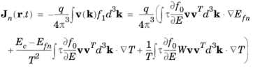
f1 must be an odd function. The electron current density can be written in the form:
Note that the definition E=Ec+W is used to split the energy terms.
The rigid band assumption is made next. This asserts that even when the bands bend, the functional form of W in k-space (measured with respect to the band edge) is unchanged. Thus
W = W(
k). Given this assumption the quantities inside the integrals are dependent only on the local band structure, except for the
df0/
dE term.
(3-59)

(3-60)

(3-61)
Qn and
μn are tensor quantities (although most semiconducting materials are cubic) so that the corresponding tensors are diagonal with identical elements and consequently can be represented by means of a scalar (cubic materials are assumed in the Semiconductor interface). Careful examination of
Equation 3-59 and
Equation 3-60 shows that these cannot straightforwardly be considered material constants because both depend on the quasi-Fermi level through the quantities
df0/dE and 1/
n. In the nondegenerate limit, the quasi-Fermi level dependence of these two quantities cancels out, since:
1/n∝exp[
-Efn/(
kBT)] and
∂f0/
∂E∝exp[
-Efn/(
kBT)]
These quantities can therefore only strictly be considered material constants in the nondegenerate limit. In the degenerate limit it is, however, possible to relate Qn to the mobility for specific models for the relaxation time (see below). In principle a mobility model could be used, which is dependent on the electron quasi-Fermi level (or the electron density) in the degenerate limit.
(3-62)
Here, the symbols introduced with the subscript change n→p have the same definitions as the electron quantities except that the relevant integrals are over the hole band.
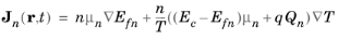
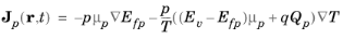
Equation 3-61 and
Equation 3-62 describe the evolution of the quasi-Fermi levels within a semiconductor. It is possible to formulate the whole equation system so that the hole and electron quasi-Fermi levels are the dependent variables. This is implemented in some of the discretization options available in the Semiconductor Module (the quasi-Fermi level formulation and the density-gradient formulation). Before deriving the more familiar drift-diffusion equations it is useful to derive the relationship between
Qn and
μn, and
Qp and
μp.
(3-63)

Since Ec (
r) is independent of
k the derivatives with respect to
E can be replaced by derivatives with respect to
W, enabling the (scalar) mobility to be written as:
where the semiclassical result v=(1/

)(
∂E(
k)/
∂k) is used and the
xx element of the mobility tensor is evaluated to compute the scalar (the
yy and
zz elements produce the same result). From
Equation 3-63:
(3-64)

In Equation 3-64 r = −1/2 corresponds to acoustic phonon scattering and
r = 3/2 is appropriate for ionized impurity scattering (
Ref. 14). In general
r can be considered a function of temperature. In COMSOL Multiphysics,
r is assumed to be
−1/2.
To transform the integral over k to an integral over
W note that
W = h2 k2 /(2m∗) so that
dk=(
m*/2
 2
2)
1/2W -1/2dW. Writing each quantity in the integral as a function of
W and rearranging gives:
(3-65)

is used. Equation 3-65 can be rewritten in the form:
(3-66)

(3-67)

Equation 3-66 and
Equation 3-67 show that
Qn can be related to
μn:
(3-68)

where the result Γ (
j + 1) =
jΓ(
j) is used.
Similarly Qp is related to
μp in exactly the same manner:
(3-69)

In COMSOL Qn and
Qp are computed from
μn and
μp using
Equation 3-68 and
Equation 3-69 with
r=−1/2. Note that in the nondegenerate limit:
Having related Qn and
Qp to the corresponding mobilities the next task is to derive equations relating the current to the carrier concentrations from
Equation 3-61 and
Equation 3-62. Once again the case of electrons is considered in detail and the results for holes are similar.
Inverting Equation 3-51 gives the following equation for the electron quasi-Fermi level:
(3-70)

where we have defined the inverse Fermi-Dirac integral (F-11/2(
α)=
η implies that
α=
F1/2(
η)). Let
α=
n/Nc and
η=
F-11/2(
α). To obtain the drift-diffusion equations
Equation 3-70 is substituted into
Equation 3-61. Note that
Nc=
Nc(
T) so that
η=F-11/2(
n/Nc)=
η(n,T). To compute the current the gradient of the quasi-Fermi level is required:
Since α=
n/Nc and
Nc∝T3/2 (
Equation 3-48):
(3-71)

In order to evaluate ∂η/∂α the result
dFn(
η)
/dη=Fn-1(
η) is required (see
Ref. 15 for details). Given this result:
(3-72)

(3-73)

where the result η = (
Efn − Ec)
/(
kBT) is used and follows from
Equation 3-70.
(3-74)

(3-75)

In the nondegenerate limit G(
α)
→1 and the following equations are obtained:
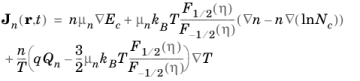
Equation 3-74 and
Equation 3-75 define the hole and electron currents used by COMSOL Multiphysics in the Semiconductor interface. To solve a model the Semiconductor interface uses these definitions in combination with Poisson’s equation and the current continuity equations.
(3-76)

(3-77)

where Un=
ΣRn,i-ΣGn,i is the net electron
recombination rate from all
generation (
Gn,i) and recombination mechanisms (
Rn,i). Similarly,
Up is the net hole recombination rate from all generation (
Gp,i) and recombination mechanisms (
Rp,i). Note that in most circumstances
Un=Up. Both of these equations follow directly from Maxwell’s equations (see
Ref. 6).
The Semiconductor interface solves Equations
3-76 and
3-77. The current densities
Jn and
Jp are given by
Equation 3-74 and
Equation 3-75, if the charge carrier dependent variables are the carrier concentrations or the log of the concentrations. For the quasi-Fermi level formulation and the density-gradient formulation,
Equation 3-61 and
Equation 3-62 are used for the current densities and the charge carrier dependent variables are the quasi-Fermi levels. For the density-gradient formulation, there are also two additional dependent variables
φn and
φp (so called Slotboom variables, SI unit: V), defined in terms of the carrier concentrations:
(3-78)