PDF

Dipole Antenna
Introduction
The dipole antenna is one of the most straightforward antenna configurations. It can be realized with two thin metallic rods that have a sinusoidal voltage difference applied between them. The length of the rods is chosen such that they are quarter wavelength elements at the operating frequency. Such an antenna has a well-known torus-like radiation pattern.
Figure 1: A dipole antenna. The model consists of two cylindrical arms of conductive material with a voltage source in between. A region of free space bounded by a perfectly matched layer (PML) surrounds the antenna.
Model Definition
The model of the antenna consists of two cylinders representing each of the dipole arms. The free space wavelength at the antenna’s operating frequency is 4 m. Thus, each of the antenna arms is 1 m long and aligned with the z-axis. The arm radius is chosen to be 0.05 m. In the limit as the radius approaches zero, this antenna approaches the analytic solution for a thin linear half wave dipole antenna.
A small cylindrical gap of size 0.01 m between the antenna arms represents the voltage source. The power supply and feed structure are not modeled explicitly, and it is assumed that a uniform voltage difference is applied across these faces. This source induces electromagnetic fields and surface currents on the adjacent conductive faces.
The dipole arm surfaces are modeled using the Impedance Boundary Condition, which is appropriate for conductive surfaces that have dimensions much larger than the skin depth. This boundary condition introduces a finite conductivity at the surface as well as resistive losses.
The air domain around the antenna is modeled as sphere of free space of radius 2 m, which is approximately the boundary between the near-field and the far-field. This sphere of air is truncated with a perfectly matched layer (PML) that acts as an absorber of outgoing radiation. The far-field pattern is computed on the boundary between the air and the PML domains.
The mesh is manually adjusted such that there are five elements per free space wavelength and that the boundaries of the antenna are meshed more finely. The PML is swept with a total of five elements along the radial direction.
Results and Discussion
The magnitude of the electric field around the antenna is shown in Figure 2. The fields appear artificially high near the excitation, as well as at the ends of the arms. These peaks in the intensity are due to local singularities; the fields at sharp transitions in the model are locally artificially high, but they do not affect the results some distance (1~2 elements) away from these regions.
The polar plot in Figure 3 of the far-field pattern in the xy-plane shows the expected isotropic radiation pattern. The 3D visualization of the far-field intensity in Figure 4 shows the expected torus-shaped pattern.
The real part of the impedance as seen by the port is evaluated to be about 120 Ω, which agrees reasonably with expectations. With further tuning of the antenna length, radius, and gap height to have the resonance at which the reactance is zero, the result approaches the well known value for a half-wave (0.48λ0) dipole antenna, which is 73 Ω.
Figure 2: A slice plot of the electric and magnetic field magnitude around the antenna.
Figure 3: The polar plot of the far field pattern in the xy-plane is isotropic.
Figure 4: A 3D visualization of the far-field pattern of the dipole shows the expected torus-shaped pattern.
Application Library path: RF_Module/Antennas/dipole_antenna
Modeling Instructions
From the File menu, choose New.
New
In the New window, click  Model Wizard.
Model Wizard
1
In the Model Wizard window, click  3D.
2
In the Select Physics tree, select Radio Frequency > Electromagnetic Waves, Frequency Domain (emw).
3
Click Add.
4
Click  Study.
5
In the Select Study tree, select General Studies > Frequency Domain.
6
Global Definitions
Parameters 1
1
In the Model Builder window, under Global Definitions click Parameters 1.
2
In the Settings window for Parameters, locate the Parameters section.
3
Study 1
Step 1: Frequency Domain
Define the study frequency ahead of performing any frequency-dependent operation such as building mesh. The physics-controlled mesh uses the specified frequency value.
1
In the Model Builder window, under Study 1 click Step 1: Frequency Domain.
2
In the Settings window for Frequency Domain, locate the Study Settings section.
3
In the Frequencies text field, type c_const/lda0.
Geometry 1
Create a sphere with a layer. The outer layer presents the PML.
Sphere 1 (sph1)
1
In the Geometry toolbar, click  Sphere.
2
In the Settings window for Sphere, locate the Size section.
3
In the Radius text field, type 2.4*arm_length.
4
Click to expand the Layers section. In the table, enter the following settings:
5
Click  Build Selected.
Choose wireframe rendering to get a better view of the interior parts.
6
Click the  Wireframe Rendering button in the Graphics toolbar.
Then, add a cylinder with layers. The top and bottom parts are the antenna radiators. A small gap between the antenna radiators is for the voltage source.
Cylinder 1 (cyl1)
1
In the Geometry toolbar, click  Cylinder.
2
In the Settings window for Cylinder, locate the Size and Shape section.
3
In the Radius text field, type r_antenna.
4
In the Height text field, type 2*arm_length+gap_size.
5
Locate the Position section. In the z text field, type -(arm_length+gap_size/2).
6
Click to expand the Layers section. In the table, enter the following settings:
7
Clear the Layers on side checkbox.
8
Select the Layers on bottom checkbox.
9
Select the Layers on top checkbox.
10
Click  Build All Objects.
Definitions
Add a perfectly matched layer on the outermost domain of the sphere.
Perfectly Matched Layer 1 (pml1)
1
In the Definitions toolbar, click  Perfectly Matched Layer.
2
3
In the Settings window for Perfectly Matched Layer, locate the Geometry section.
4
From the Type list, choose Spherical.
View 1
Suppress some domains and boundaries. This helps to see the interior parts when setting up the physics and reviewing the mesh.
Hide for Physics 1
1
In the Model Builder window, right-click View 1 and choose Hide for Physics.
2
Hide for Physics 2
1
Right-click View 1 and choose Hide for Physics.
2
In the Settings window for Hide for Physics, locate the Geometric Entity Selection section.
3
From the Geometric entity level list, choose Boundary.
4
Materials
Assign air as the material for all domains and override the antenna radiator surface with copper.
Add Material
1
In the Materials toolbar, click  Add Material to open the Add Material window.
2
Go to the Add Material window.
3
In the tree, select Built-in > Air.
4
Click the Add to Component button in the window toolbar.
5
In the tree, select Built-in > Copper.
6
Click the Add to Component button in the window toolbar.
7
In the Materials toolbar, click  Add Material to close the Add Material window.
Materials
Copper (mat2)
1
In the Settings window for Material, locate the Geometric Entity Selection section.
2
From the Geometric entity level list, choose Domain.
3
Electromagnetic Waves, Frequency Domain (emw)
Lumped Port 1
1
In the Physics toolbar, click  Boundaries and choose Lumped Port.
2
Click the  Zoom In button in the Graphics toolbar, a couple of times to see the small gap between antenna radiators clearly.
3
4
In the Settings window for Lumped Port, locate the Lumped Port Properties section.
5
From the Type of lumped port list, choose User defined.
6
In the hport text field, type gap_size.
7
In the wport text field, type 2*pi*r_antenna.
8
Specify the ah vector as
For the first port, wave excitation is on by default.
Electromagnetic Waves, Frequency Domain (emw)
Next, to set up the physics quickly, utilize the toolbar buttons that you find at the top of the physics interface’s Settings window.
1
In the Model Builder window, under Component 1 (comp1) click Electromagnetic Waves, Frequency Domain (emw).
2
In the Settings window for Electromagnetic Waves, Frequency Domain, click the Lossy Features from Materials button in the window toolbar. This tool automatically generates or updates lossy features, including impedance boundary, domain impedance boundary, or transition boundary conditions, adjusting the selection based on material definitions, geometry size, and skin depth.
Impedance Boundary Condition 1
1
Click the  Zoom Extents button in the Graphics toolbar.
2
Click the  Zoom Extents button in the Graphics toolbar.
Far-Field Domain 1
In the Physics toolbar, click  Domains and choose Far-Field Domain.
Mesh 1
In the Model Builder window, under Component 1 (comp1) right-click Mesh 1 and choose Build All.
Study 1
In the Study toolbar, click  Compute.
Results
The default plot shows the E-field norm, the 2D far field in a polar plot, and the 3D far-field radiation pattern.
Multislice
1
In the Model Builder window, expand the Results > Electric Field (emw) node, then click Multislice.
2
In the Settings window for Multislice, locate the Multiplane Data section.
3
Find the X-planes subsection. In the Planes text field, type 0.
4
Find the Z-planes subsection. In the Planes text field, type 0.
5
Click to expand the Range section. Select the Manual color range checkbox.
6
In the Maximum text field, type 20.
7
Locate the Coloring and Style section. From the Color table list, choose JupiterAuroraBorealis.
8
In the Electric Field (emw) toolbar, click  Plot.
9
Click the  Zoom In button in the Graphics toolbar.
Arrow Volume 1
1
In the Model Builder window, right-click Electric Field (emw) and choose Arrow Volume.
2
In the Settings window for Arrow Volume, locate the Arrow Positioning section.
3
Find the X grid points subsection. In the Points text field, type 21.
4
Find the Y grid points subsection. In the Points text field, type 1.
5
Find the Z grid points subsection. In the Points text field, type 21.
6
Locate the Coloring and Style section. From the Arrow length list, choose Logarithmic.
7
In the Range quotient text field, type 3000.
8
From the Color list, choose White.
Slice 1
1
Right-click Electric Field (emw) and choose Slice.
2
In the Settings window for Slice, locate the Expression section.
3
In the Expression text field, type 20*log10(emw.normH).
4
Locate the Plane Data section. From the Plane list, choose XY-planes.
5
In the Planes text field, type 1.
6
Locate the Coloring and Style section. From the Color table list, choose Thermal.
7
From the Color table transformation list, choose Reverse.
Transparency 1
1
Right-click Slice 1 and choose Transparency.
2
In the Settings window for Transparency, locate the Transparency section.
3
Set the Transparency value to 0.25.
Electric Field (emw)
1
In the Model Builder window, under Results click Electric Field (emw).
2
In the Settings window for 3D Plot Group, click to expand the Selection section.
3
From the Geometric entity level list, choose Domain.
4
5
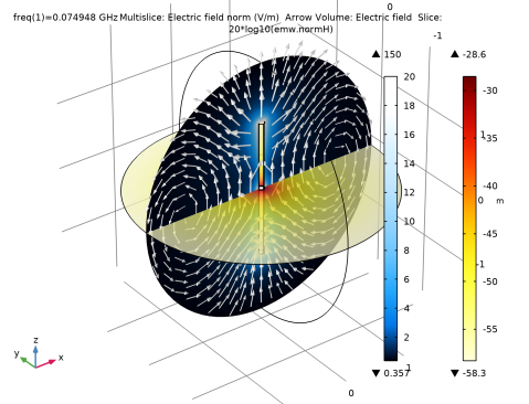
Select the Apply to dataset edges checkbox.
6
In the Electric Field (emw) toolbar, click  Plot.
The results show the E-field norm and dB-scaled magnetic field norm distribution around the antenna radiators. It is plotted in Figure 2.
Electric Field, Logarithmic (emw)
In the Model Builder window, click Electric Field, Logarithmic (emw).
2D Far Field (emw)
Adjust the axis range.
1
In the Model Builder window, click 2D Far Field (emw).
2
In the Settings window for Polar Plot Group, locate the Axis section.
3
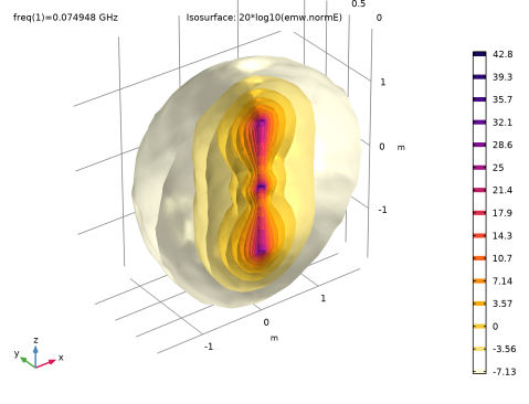
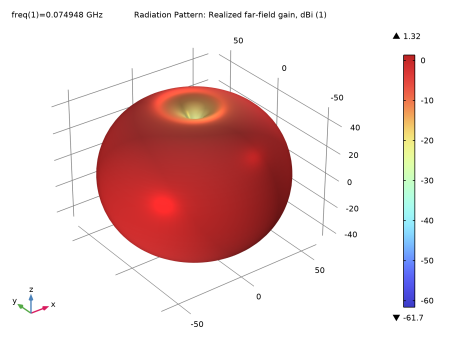
Select the Manual axis limits checkbox.
4
In the r minimum text field, type -20.
5
In the r maximum text field, type 0.
Radiation Pattern 1
1
In the Model Builder window, expand the 2D Far Field (emw) node, then click Radiation Pattern 1.
2
In the Settings window for Radiation Pattern, locate the Expression section.
3
In the Expression text field, type emw.normdBEfar.
4
Click to expand the Legends section. From the Legends list, choose Manual.
5
6
In the 2D Far Field (emw) toolbar, click  Plot.
The plotted H-plane pattern is omnidirectional (isotropic) on the xy-plane as shown in Figure 3. The E- and H-plane of a linearly polarized antenna are defined by the antenna main polarization. The E-plane includes the main polarization that is Ez in this model while the H-plane is perpendicular to the main polarization.
Radiation Pattern 2
1
Right-click Results > 2D Far Field (emw) > Radiation Pattern 1 and choose Duplicate.
2
In the Settings window for Radiation Pattern, locate the Evaluation section.
3
Find the Normal vector subsection. In the y text field, type 1.
4
In the z text field, type 0.
5
Find the Angles subsection. From the Compute beamwidth list, choose On.
6
In the Level down text field, type 3.
With these settings, the beamwidth is calculated according to the given level-down value.
7
Locate the Legends section. In the table, enter the following settings:
8
In the 2D Far Field (emw) toolbar, click  Plot.
The computed half-power beamwidth is about 75.5 degrees. Note that the result is valid only when the main beam for calculation is at 0 degree in the plot. The beam orientation in the plot can be adjusted by setting the Normal vector and Reference direction.
3D Far Field, Gain (emw)
1
In the Model Builder window, under Results click 3D Far Field, Gain (emw).
Compare the reproduced plot with Figure 4.
Evaluate the port impedance.
Global Evaluation 2
1
In the Results toolbar, click  Global Evaluation.
2
In the Settings window for Global Evaluation, click Replace Expression in the upper-right corner of the Expressions section. From the menu, choose Component 1 (comp1) > Electromagnetic Waves, Frequency Domain > Ports > emw.Zport_1 - Lumped port 1 impedance - Ω.
3
Click  Evaluate.
3D Plot Group 5
In the Results toolbar, click  3D Plot Group.
Isosurface 1
1
Right-click 3D Plot Group 5 and choose Isosurface.
2
In the Settings window for Isosurface, locate the Expression section.
3
In the Expression text field, type 20*log10(emw.normE).
4
Locate the Levels section. In the Total levels text field, type 15.
5
Locate the Coloring and Style section. From the Color table list, choose HeatCamera.
6
From the Color table transformation list, choose Reverse.
Filter 1
1
Right-click Isosurface 1 and choose Filter.
2
In the Settings window for Filter, locate the Element Selection section.
3
In the Logical expression for inclusion text field, type y>0.
Selection 1
1
In the Model Builder window, right-click Isosurface 1 and choose Selection.
2
3
In the 3D Plot Group 5 toolbar, click  Plot.
3D Plot Group 5
1
In the Model Builder window, under Results click 3D Plot Group 5.
2
In the Settings window for 3D Plot Group, locate the Plot Settings section.
3
Clear the Plot dataset edges checkbox.
4
In the 3D Plot Group 5 toolbar, click  Plot.