You are viewing the documentation for an older COMSOL version. The latest version is
available here.
Use the Port node where electromagnetic energy enters or exits the model. A port can launch and absorb specific modes. Use the boundary condition to specify wave type ports. Ports support S-parameter calculations but can be used just for exciting the model. This node is not available with the Electromagnetic Waves, Transient interface.
|
•
|
Circular Port Reference Axis to determine a reference direction for the modes. This subnode is selected from the Points submenu when Circular is selected as the type of port.
|
|
•
|
Periodic Port Reference Point to uniquely determine reciprocal lattice vectors. This subnode is selected from the Points submenu when Periodic is selected as the type of port.
|
When Transverse electromagnetic (TEM) is selected as the type of port, the following subnodes are available from the context menu, by right-clicking the
Port node, or from the
Physics toolbar,
Attributes menu:
|
•
|
Ground to define zero potential boundaries for the port mode field calculation in TEM Boundary Mode Analysis.
|
|
•
|
Electric Potential to define positive or negative 1 V potential boundaries for the port mode field calculation in TEM Boundary Mode Analysis.
|
Enter a unique Port name. Only nonnegative integer numbers can be used as
Port name as it is used to define the elements of the S-parameter matrix and numeric port names are also required for port sweeps and Touchstone file export.
Select the Type of Port —
User defined,
Numeric,
Transverse electromagnetic (TEM),
Rectangular,
Coaxial,
Circular, or
Periodic.
Periodic ports are available in 3D and 2D.
Circular and
Coaxial ports are available in 3D and 2D axisymmetry.
Numeric ports require a
Boundary Mode Analysis study type. It should appear before the frequency domain study node in the study branch of the model tree. If more than one numeric port is needed, use one Boundary Mode Analysis node per port and assign each to the appropriate port. Then, it is best to add all the studies; Boundary Mode Analysis 1, Boundary Mode Analysis 2, …, Frequency Domain 1, manually.
Numeric ports are by default computed for the deformed mesh whereas other types of ports compute the mode shape using geometry information.
|
|
The Boundary Mode Analysis study step stores the frequency fref and propagation constant βref for which it was run. For a TE, TM, or TEM mode, the propagation constant β for an arbitrary frequency f is given by
In addition, for TE, TM, and TEM modes, the mode field shape is independent of the frequency. Thus, when making a frequency sweep including only TE, TM, and TEM modes, the Boundary Mode Analysis study steps can be done for just one frequency, with the propagation constants obtained from the expression above for the other frequencies. For waveguides consisting of multiple dielectric materials, like optical fibers, where there are no TE, TM, or, TEM modes, the Boundary Mode Analysis steps must be recomputed for each frequency.
|
Transverse electromagnetic (TEM) ports require a
TEM Boundary Mode Analysis study type. It should appear before the frequency domain study node in the study branch of the model tree. Add Ground and Electric Potential subnodes to compute the port mode field and impedance. These subnodes are available from the context menu (right-click the Port parent node) or from the
Physics toolbar,
Attributes menu. Enter a
Characteristic impedance Zref (SI unit:
Ω). The default is 50
Ω. The characteristic impedance of a port is calculated using the square root of the ratio of the inductance and capacitance. The electric mode field on a port boundary is scaled by the ratio between the computed mode characteristic impedance and
Zref.
To set whether it is an inport or a listener port, select On or
Off from the
Wave excitation at this port list. If
On is selected, enter a
Port input power Pin (SI unit: W in 3D and 2D axisymmetry and W/m in 2D) or a
Deposited power Pdep (SI unit: W in 3D and 2D axisymmetry and W/m in 2D) if the
Enable active port feedback check box is marked. When a
Deposited power is specified, the input power is adjusted so that the power that is not reflected equals the specified
Deposited power. If
Enable active port feedback is marked this must be the only inport.
|
|
The Port Sweep Settings section in the Electromagnetic Waves, Frequency Domain interface cycles through the ports, computes the entire S-matrix and exports it to a Touchstone file. When using port sweeps, the local setting for Wave excitation at this port is overridden by the solver so only one port at a time is excited.
|
Select the Activate slit condition on interior port check box to use the
Port boundary condition on interior boundaries.
Then select a Slit type —
PEC-backed (the default) or
Domain-backed. The
PEC-backed type makes the port on interior boundaries perform as it does on exterior boundaries. The
Domain-backed type can be combined with perfectly matched layers to absorb the excited mode from a source port and other higher order modes.
Click Toggle Power Flow Direction button to define the power flow for the port. For an excited port, the power flow should point in to the excited domain and for a listener port the power flow should point out from the excited domain. The power flow direction is visualized with a red arrow on the port boundary in the Graphics window.
|
|
When the Slit type is set to Domain-backed, there must be no waves reflected from the domain backing the port. Thus, the backing domain must have homogeneous material and geometric properties and it should be truncated by a PML domain or a nonreflecting boundary condition.
|
When analyzing an arbitrary shape of a port, if the port boundary consists of at least two separate conducting parts, the port can support a (quasi-) TEM mode. In this case, it is possible to calculate the port mode characteristic impedance from the results of a Boundary Mode Analysis and include the impedance mismatch compared to the user-specified reference impedance in the simulation by selecting the
Analyze as a TEM field check box. The
Analyze as a TEM field requires an
Integration Line for Voltage subfeature to calculate the port mode impedance. The
Integration Line for Current subfeature is optional. The impedance is calculated using either the ratio of the voltage and current when both
Integration Line for Voltage and
Integration Line for Current are defined, or deduced from the voltage and power when only the
Integration Line for Voltage is defined. These subfeatures are available from the context menu (right-click the Port parent node) or from the
Physics toolbar,
Attributes menu.
Enter a reference Characteristic impedance Zref (SI unit:
Ω). The default is 50
Ω. The mode field on a port boundary is scaled by the ratio between the computed characteristic impedance and user-specified
Zref.
The input is based on the Type of Port selected above —
User Defined,
Rectangular,
Circular, or
Periodic. No entry is required if
Numeric or
Coaxial are selected.
Set the Mode phase θin (SI unit: rad) for the port mode field. The default is 0 radians. For instance, if the inspected port mode field is polarized in the opposite direction compared to the expected direction, a
Mode phase of
π (enter
pi in the field) can be used for polarizing the mode field in the expected direction. Notice that a change of the
Mode phase, either on the exciting or the listener port, changes also the S-parameter coupling the exciting and the listener port. However, a change of the
Mode phase on the exciting port does not modify the reflection coefficient (normally denoted S11) associated with the exciting port.
For User defined specify the eigenmode of the outgoing wave at the port. Even if
Wave excitation at this port is set to
On, the mode field should represent the outgoing wave. The mode field can be entered with an arbitrary amplitude and is normalized internally.
|
•
|
Enter the components of the Electric mode field E0 (SI unit: V/m) or the Magnetic mode field H0 (SI unit: A/m). The entered expressions must be differentiable.
|
|
•
|
Enter the Propagation constant β (SI unit: rad/m). This is frequency dependent for all but TEM modes and a correct frequency-dependent expression must be used.
|
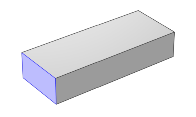
The following figure shows an example of a boundary selection for a Rectangular waveguide port in a 3D model. The mode field is assigned to this selection.

For Rectangular specify a unique rectangular mode.
For 3D components, select a Mode type —
Transverse electric (TE) or
Transverse magnetic (TM). Enter the
Mode number, for example, 10 for a TE
10 mode, or 11 for a TM
11 mode. When the port boundaries are parallel to one of the Cartesian coordinate planes, click the
Plot Analytical Port Mode Field button to inspect the mode field instantly before running a simulation.
For 2D components, to excite the fundamental mode, select the mode type Transverse electromagnetic (TEM), since the rectangular port represents a parallel-plate waveguide port that can support a TEM mode. Only TE modes are possible when solving for the out-of-plane vector component, and only TM and TEM modes are possible when solving for the in-plane vector components. There is only a single mode number, which is selected from a list.
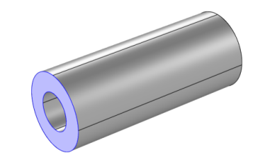
The following figure shows an example of a boundary selection for a Coaxial waveguide port in a 3D model. The mode field is assigned to this selection.

Coaxial only supports
Transverse electromagnetic (TEM) mode type. When the port boundaries are parallel to one of the Cartesian coordinate planes, click the
Plot Analytical Port Mode Field button to inspect the mode field instantly before running a simulation.
In 2D axisymmetry, Coaxial does not support nonzero azimuthal mode number. The
Azimuthal mode number in the
Physics interface should be defined as zero.
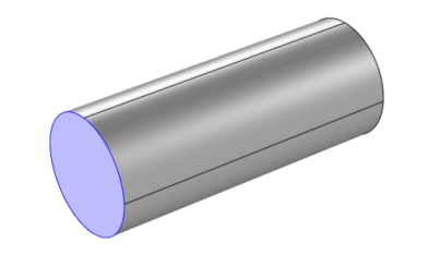
The following figure shows an example of a boundary selection for a Circular waveguide port in a 3D model. The mode field is assigned to this selection.

For Circular specify a unique circular mode.
|
•
|
Select a Mode type — Transverse electric (TE) or Transverse magnetic (TM).
|
For 3D components, enter the Mode number, for example, 11 for a TE
11 mode, or 01 for a TM
01 mode. When
Circular is selected as the type of port in 3D, the
Circular Port Reference Axis subnode is available from the context menu (right-click the parent node) or from the
Physics toolbar,
Attributes menu. It defines the orientation of fields on a port boundary. When the port boundaries are parallel to one of the Cartesian coordinate planes, click the
Plot Analytical Port Mode Field button to inspect the mode field instantly before running a simulation.
For 2D axisymmetry components, select whether the Azimuthal mode number is defined in the
Physics interface or if it is
User defined. For
User defined define an integer constant or an integer parameter expression for the
Azimuthal mode number. Note that the absolute value of the
Azimuthal mode number must be less than 11.
For Periodic, specify parameters for the mode field. When
Periodic is selected, the
Diffraction Order port subnode is available from the context menu (right-click the parent node) or from the
Physics toolbar,
Attributes menu.
Select an Input quantity —
Electric field or
Magnetic field — and define the mode field amplitude for the outgoing wave at the port. Even if
Wave excitation at this port is set to
On, the mode field amplitude should represent the outgoing wave that corresponds to the actual incoming wave.
|
•
|
For 2D components and if the Input quantity is set to Electric field, define the Electric mode field amplitude. For example, for a TE wave set the x, y, and z components to 0, 0, 1. Similarly, if the Input quantity is set to Magnetic field, define the Magnetic mode field amplitude. For a TM wave set the x, y, and z components to 0, 0, and 1.
|
|
•
|
Define the Angle of incidence, if Wave excitation at this port is On.
|
For 3D components, if Wave excitation at this port is
On, define the
Elevation angle of incidence and
Azimuth angle of incidence. The
Elevation angle of incidence α1 and
Azimuth angle of incidence α2 are used in the relations
where k is the wave vector,
kparallel is the projection of
k onto the port,
kF is the k-vector for Floquet periodicity,
n is the outward unit normal vector to the boundary, and

is one of the normalized primitive unit cell vectors from the periodic structure defined from
Periodic Port Reference Point.
The Elevation angle of incidence α1 is the angle between
n and
k.
The Azimuth angle of incidence is the counterclockwise rotating angle from the primitive vector
a1 around the axis built with
Periodic Port Reference Point and
n.
For periodic ports with hexagonal port boundaries, the definition of the vector a1 is slightly different from the default definition. In this case, the unit cell is actually a rhomboid, with primitive vectors pointing in other directions than the side vectors of the hexagon. Thus, for a hexagonal periodic port, the vector
a1 is defined along one of the sides of the hexagon, and it is not one of the primitive vectors of the hexagonal point lattice. The
Azimuth angle of incidence α2 is still measured from the vector
a1, even though this vector now refers to a side vector of the hexagonal port boundary and not a primitive vector.
For 2D components define the Angle of incidence. The
Angle of incidence α is defined by the relation
where k is the projection of the wave vector in the
xy-plane,
n is the normalized normal vector to the boundary,
k is the magnitude of the projected wave vector in the
xy-plane, and
z is the unit vector in the
z direction.
|
|
The propagation directions for listener Periodic ports are deduced from the angle setting(s) for the source Periodic port and the refractive indices defined for the source and the listener ports. Thus, adding source Periodic ports with different propagation angles will give ambiguous propagation directions for the listener Periodic ports.
|
Default Polarization plots are automatically generated for Periodic ports in 3D and in 2D, if the
Electric field components solved for setting in the
Components section for the physics interface is set to
Three-component vector. The Polarization plot includes polarization ellipses for each diffraction order. The polarization ellipse line graphs are generated by plotting the in-plane Jones vector element versus the out-of-plane Jones vector element.
This section is only available for Periodic ports to provide parameter settings that are used when automatically adding
Diffraction Order subnodes to
Periodic ports.
|
•
|
Select the Include in automatic diffraction order calculation check box to add Diffraction Order subnodes to the selected Periodic port, when the Add Diffraction Orders button is clicked from the exciting Periodic port.
|
|
•
|
Define the Refractive index, real part at the boundary.
|
|
•
|
Define the Maximum frequency — From study (the default) or User defined. When From study is selected, the Maximum frequency is taken from the study step associated with the physics interface. For User defined, enter the maximum frequency fmax (SI unit: Hz). The default value is 0 Hz. If a single frequency is used, insert the frequency, or if a frequency sweep is performed, insert the maximum frequency of the sweep. This parameter is only available when Wave excitation at this port is On.
|
When all parameters are defined, click the Add Diffraction Orders button from the exciting
Periodic port to automatically create
Diffraction Order ports as subnodes to all
Periodic ports having the
Include in automatic diffraction order calculation check box selected.
|
|
Perform the same action as when clicking the Add Diffraction Orders button, using the COMSOL API, with the Java code
model.component("comp1").physics("ewfd").feature("port1").runCommand("addDiffractionOrders");
where “comp1”, “ewfd”, and “port1” are the tags for the model component, the physics interface, and the excited port, respectively, and model is a model object.
|
This utility is available for Rectangular and
Circular port types. Enter a
Relative permittivity (default is 1) of the material fully filled in a waveguide and then click the
Compute Waveguide Cutoff Frequency button to compute the cutoff frequency for the particular waveguide geometry and the selected
Mode type. The result is displayed in the
Messages window.
Set the Port Offset doffset (SI unit: m) for the de-embedded S-parameter calculation. The default is 0 m. The phase of the de-embedded S-parameters is adjusted from the calculated S-parameters with the propagation constant and the value of
doffset. The full expression for the de-embedded S-parameter is given by
where m is the source port name,
n is the listener port name,
β is the propagation constant, and
d is the offset distance from the port boundary. The generated variables are typically denoted by
emw.dS11 and
emw.dS21.
The de-embedding functionality is triggered when doffset is set to a nonzero value. It is assumed that the domain between the port boundary and the boundary projected by the
doffset is straight, while maintaining a constant cross-sectional shape.
To display this section, click the Show More Options button (

) and select
Advanced Physics Options in the
Show More Options dialog box. For information about the
Constraint Settings section, see
Constraint Settings in the
COMSOL Multiphysics Reference Manual.
