PDF

Radome with Double-Layered Dielectric Lens
Introduction
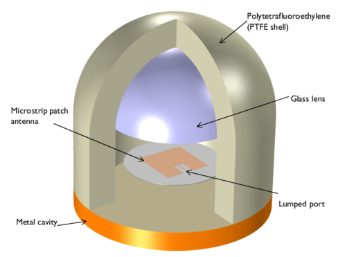
A radome is an enclosure for protecting an antenna from the environment. It should be almost completely RF transparent, and can be designed to improve radiation characteristics such as antenna directivity. Here a radome, as shown in Figure 1, improves the gain of a patch antenna.
Figure 1: A microstrip patch antenna enclosed by dielectric medium. A double-layered dielectric lens is placed at the boresight of the antenna and confines the fields to increase the antenna gain.
Model Definition
The model shown in Figure 1 represents the radome enclosing a patch antenna. The patch antenna is a thin layer of metal, sitting on a circular dielectric above a ground plane. The antenna and ground plane are modeled as infinitely thin perfect electric conductor (PEC) surfaces. The antenna itself is fed by a 50 Ω lumped port, representing a feed from the power source.
The entire structure is enclosed in a cylindrical PTFE housing, capped by a half-spherical shell. Within this, a half-sphere of a quartz glass dielectric is used to increase the antenna gain. The PTFE housing is backed by a metal housing, also modeled as PEC surfaces. The structure is designed to operate at 1.632 GHz.
The entire antenna structure is modeled within a sphere with the properties of vacuum. This sphere is truncated by a perfectly matched layer (PML) domain that acts as a boundary to free space. The distance from the antenna to the PML is a variable that does require some study. The PML should not be within the reactive near-field region of the antenna structure. However, the size of the reactive near field is not strictly definable, so the distance from the antenna to the PML should be studied for each model. The thickness of the PML itself is not critical, and can be made approximately one tenth of the air sphere diameter.
The meshing of radiating structures requires some care. As a rule of thumb, use at least five elements per wavelength in each material, although if absolutely necessary, as few as three elements can do. Furthermore, curved edges and surfaces should be meshed with at least two elements per 90° chord, and the stricter of the two criteria should always be used. Additionally, tetrahedral elements of approximately unit aspect ratio are preferable in most modeling regions, with the exception of the PML domains. Because the PML domain preferentially absorbs radiated energy in one direction, the mesh should conform to this. A swept mesh is thus recommended in PML regions.
Results and Discussion
The far-field radiation pattern is shown in Figure 2. The observed radiation pattern is more directive than that of a patch antenna only. Figure 4 shows E-fields that are confined through the radome structure, which results in stronger fields at the center of the top shell. This example model shows that a radome can work as an antenna enclosure and improve the antenna directivity.
Figure 2: Far-field radiation pattern at the E-plane (blue) and the H-plane (green) at 1.632 GHz. The radiation pattern is more directive than that of a patch antenna.
Figure 3: The 3D far-field radiation pattern is directive toward the front side of the radome.
Figure 4: E-field distribution on the radome shell. Note the strong fields at the center of the top radome shell.
References
1. D.M. Pozar, Microwave Engineering, John Wiley & Sons, 1998.
2. M. Skolnik, Introduction to Radar Systems, McGraw-Hill, 1980.
3. F.T. Ulaby, Fundamentals of Applied Electromagnetics, Prentice Hall, 1997.
Application Library path: RF_Module/Antennas/radome_antenna
Modeling Instructions
From the File menu, choose New.
New
In the New window, click  Model Wizard.
Model Wizard
1
In the Model Wizard window, click  3D.
2
In the Select Physics tree, select Radio Frequency>Electromagnetic Waves, Frequency Domain (emw).
3
Click Add.
4
Click  Study.
5
In the Select Study tree, select General Studies>Frequency Domain.
6
Study 1
Step 1: Frequency Domain
1
In the Model Builder window, under Study 1 click Step 1: Frequency Domain.
2
In the Settings window for Frequency Domain, locate the Study Settings section.
3
In the Frequencies text field, type 1.62[GHz].
Global Definitions
Parameters 1
1
In the Model Builder window, under Global Definitions click Parameters 1.
2
In the Settings window for Parameters, locate the Parameters section.
3
Click  Load from File.
4
mil refers to the unit milliinch. The evaluated impedance of the 1.13 mm feed line on a 20 mil substrate is approximately 50Ω.
Geometry 1
1
In the Model Builder window, under Component 1 (comp1) click Geometry 1.
2
In the Settings window for Geometry, locate the Units section.
3
From the Length unit list, choose mm.
First, create a block for the patch.
Patch
1
In the Geometry toolbar, click  Block.
2
In the Settings window for Block, type Patch in the Label text field.
3
Locate the Size and Shape section. In the Width text field, type w_patch.
4
In the Depth text field, type l_patch.
5
In the Height text field, type thickness.
6
Locate the Position section. From the Base list, choose Center.
7
In the z text field, type -40.
8
Click  Build Selected.
Add a block for the tuning stub.
Stub
1
In the Geometry toolbar, click  Block.
2
In the Settings window for Block, type Stub in the Label text field.
3
Locate the Size and Shape section. In the Width text field, type w_tuning.
4
In the Depth text field, type l_tuning.
5
In the Height text field, type thickness.
6
Locate the Position section. From the Base list, choose Center.
7
In the x text field, type w_tuning/2+w_line/2.
8
In the y text field, type l_tuning/2-25.
9
In the z text field, type -40.
10
Click  Build Selected.
Copy the tuning stub. A pair of the tuning stubs is symmetric with respect to the feed line.
Copy 1 (copy1)
1
In the Geometry toolbar, click  Transforms and choose Copy.
2
3
In the Settings window for Copy, locate the Displacement section.
4
In the x text field, type -w_tuning-w_line.
5
Click  Build Selected.
Subtract the tuning stubs from the patch. This action creates the 50Ω feed line, too.
Difference 1 (dif1)
1
In the Geometry toolbar, click  Booleans and Partitions and choose Difference.
2
3
In the Settings window for Difference, locate the Difference section.
4
Find the Objects to subtract subsection. Click to select the  Activate Selection toggle button.
5
Select the objects blk2 and copy1 only.
6
Click  Build Selected.
Add a cylinder for the substrate.
Substrate
1
In the Geometry toolbar, click  Cylinder.
2
In the Settings window for Cylinder, type Substrate in the Label text field.
3
Locate the Size and Shape section. In the Radius text field, type 50.
4
In the Height text field, type thickness.
5
Locate the Position section. In the z text field, type -40-thickness/2.
6
Click  Build Selected.
7
Click the  Zoom Extents button in the Graphics toolbar.
Create a sphere for the double-layered dielectric lens.
Radome
1
In the Geometry toolbar, click  Sphere.
2
In the Settings window for Sphere, type Radome in the Label text field.
3
Locate the Size section. In the Radius text field, type r_radome.
4
Locate the Position section. In the z text field, type 15.
5
Click to expand the Layers section. In the table, enter the following settings:
6
Click  Build Selected.
7
Click the  Wireframe Rendering button in the Graphics toolbar.
8
Click the  Zoom Extents button in the Graphics toolbar.
Add a block to cut the bottom half of the above sphere.
Cut Bottom Half
1
In the Geometry toolbar, click  Block.
2
In the Settings window for Block, type Cut Bottom Half in the Label text field.
3
Locate the Size and Shape section. In the Width text field, type r_radome*2.5.
4
In the Depth text field, type r_radome*2.5.
5
In the Height text field, type r_radome*2.
6
Locate the Position section. From the Base list, choose Center.
7
In the z text field, type -85.
8
Click  Build Selected.
Create a hemisphere by subtracting the above block from the dielectric lens sphere.
Radome Top
1
In the Geometry toolbar, click  Booleans and Partitions and choose Difference.
2
In the Settings window for Difference, type Radome Top in the Label text field.
3
4
Locate the Difference section. Find the Objects to subtract subsection. Click to select the  Activate Selection toggle button.
5
6
Click  Build Selected.
Create a cylinder with a layer for the side wall of the radome.
Radome Wall
1
In the Geometry toolbar, click  Cylinder.
2
In the Settings window for Cylinder, type Radome Wall in the Label text field.
3
Locate the Size and Shape section. In the Radius text field, type r_radome.
4
In the Height text field, type h_radome_wall.
5
Locate the Position section. In the z text field, type -65.
6
Click to expand the Layers section. In the table, enter the following settings:
7
Click  Build Selected.
Create a cylinder for the bottom part of the radome.
Radome Bottom
1
In the Geometry toolbar, click  Cylinder.
2
In the Settings window for Cylinder, type Radome Bottom in the Label text field.
3
Locate the Size and Shape section. In the Radius text field, type r_radome.
4
In the Height text field, type t_radome_bottom.
5
Locate the Position section. In the z text field, type -85.
6
Click  Build Selected.
Create a sphere for the PMLs.
PMLs
1
In the Geometry toolbar, click  Sphere.
2
In the Settings window for Sphere, type PMLs in the Label text field.
3
Locate the Size section. In the Radius text field, type 190.
4
Locate the Layers section. In the table, enter the following settings:
5
Click  Build All Objects.
Definitions
Add a selection for the radome.
Radome
1
In the Definitions toolbar, click  Explicit.
2
In the Settings window for Explicit, type Radome in the Label text field.
3
These are the visible domains from the default 3D view. Domain 7 and 9 are hidden in this figure.
Perfectly Matched Layer 1 (pml1)
1
In the Definitions toolbar, click  Perfectly Matched Layer.
2
3
In the Settings window for Perfectly Matched Layer, locate the Geometry section.
4
From the Type list, choose Spherical.
Hide some boundaries and domains to get a better view of the interior parts.
Definitions
Hide for Physics 1
1
In the Model Builder window, right-click View 1 and choose Hide for Physics.
2
Hide for Physics 2
1
Right-click View 1 and choose Hide for Physics.
2
Hide for Physics 3
1
Right-click View 1 and choose Hide for Physics.
2
In the Settings window for Hide for Physics, locate the Geometric Entity Selection section.
3
From the Geometric entity level list, choose Boundary.
4
Click  Paste Selection.
5
In the Paste Selection dialog box, type 9-10, 17, 24, 26, 29-30, 50-51, 54, 58-60 in the Selection text field.
6
Electromagnetic Waves, Frequency Domain (emw)
Perfect Electric Conductor 2
1
In the Model Builder window, under Component 1 (comp1) right-click Electromagnetic Waves, Frequency Domain (emw) and choose the boundary condition Perfect Electric Conductor.
2
In the Settings window for Perfect Electric Conductor, locate the Boundary Selection section.
3
Click  Paste Selection.
4
In the Paste Selection dialog box, type 13-15, 34, 38-39, 52, 79 in the Selection text field.
5
Far-Field Domain 1
In the Physics toolbar, click  Domains and choose Far-Field Domain.
Lumped Port 1
1
In the Physics toolbar, click  Boundaries and choose Lumped Port.
2
For the first port, wave excitation is on by default.
Zoom to see the port boundary clearly.
Materials
Assign material properties on the model. First, set all domains with the built-in air.
Add Material
1
In the Home toolbar, click  Add Material to open the Add Material window.
2
Go to the Add Material window.
3
4
Click Add to Component in the window toolbar.
Materials
Override the substrate with the dielectric material of εr = 3.38.
Substrate
1
In the Model Builder window, under Component 1 (comp1) right-click Materials and choose Blank Material.
2
In the Settings window for Material, type Substrate in the Label text field.
3
4
Locate the Material Contents section. In the table, enter the following settings:
Override the radome with the PTFE material.
PTFE
1
Right-click Materials and choose Blank Material.
2
In the Settings window for Material, type PTFE in the Label text field.
3
Locate the Geometric Entity Selection section. From the Selection list, choose Radome.
4
Locate the Material Contents section. In the table, enter the following settings:
Then, override the lens with glass. Choose from the material library.
Add Material
1
Go to the Add Material window.
2
In the tree, select Built-in>Glass (quartz).
3
Click Add to Component in the window toolbar.
4
In the Home toolbar, click  Add Material to close the Add Material window.
Materials
Glass (quartz) (mat4)
Select Domain 12 only.
Mesh 1
1
In the Model Builder window, under Component 1 (comp1) right-click Mesh 1 and choose Build All.
2
Click the  Zoom In button in the Graphics toolbar.
Study 1
In the Home toolbar, click  Compute.
Results
Electric Field (emw)
Begin the results analysis and visualization by modifying the first default plot to show the dB-scaled E-field norm in the xz-plane.
Multislice
1
In the Model Builder window, expand the Electric Field (emw) node, then click Multislice.
2
In the Settings window for Multislice, locate the Expression section.
3
In the Expression text field, type 20*log10(emw.normE).
4
Locate the Multiplane Data section. Find the Z-planes subsection. In the Planes text field, type 0.
5
Find the X-planes subsection. In the Planes text field, type 0.
6
Find the Y-planes subsection. From the Entry method list, choose Coordinates.
7
In the Coordinates text field, type 0.
8
In the Electric Field (emw) toolbar, click  Plot.
9
Click the  Zoom Extents button in the Graphics toolbar.
10
Click the  Zoom In button in the Graphics toolbar.
The shape of the field pattern is similar to the H-plane radiation pattern.
Adjust the polar plot settings to visualize the far-field pattern on the E-plane.
Radiation Pattern 1
1
In the Model Builder window, expand the Results>2D Far Field (emw) node, then click Radiation Pattern 1.
2
In the Settings window for Radiation Pattern, locate the Evaluation section.
3
Find the Angles subsection. In the Number of angles text field, type 100.
4
Find the Reference direction subsection. In the x text field, type 0.
5
In the y text field, type 1.
6
Find the Normal vector subsection. In the x text field, type 1.
7
In the z text field, type 0.
8
In the 2D Far Field (emw) toolbar, click  Plot.
The E-plane in this model is located on the yz-plane where φ is measured counterclockwise from the y-axis.
Add the H-plane polar plot.
Radiation Pattern 2
1
Right-click Results>2D Far Field (emw)>Radiation Pattern 1 and choose Duplicate.
2
In the Settings window for Radiation Pattern, locate the Evaluation section.
3
Find the Reference direction subsection. In the x text field, type 1.
4
In the y text field, type 0.
5
Find the Normal vector subsection. In the x text field, type 0.
6
In the y text field, type -1.
7
In the 2D Far Field (emw) toolbar, click  Plot.
The H-plane is located on the xz-plane where φ is measured counterclockwise from the x-axis.
Compare the resulting plot with that shown in Figure 2.
3D Far Field, Gain (emw)
Compare the 3D far-field radiation pattern plot with Figure 3.
Create a selection of the solution to visualize the E-field only on the radome.
Study 1/Solution 1 (2) (sol1)
In the Results toolbar, click  More Datasets and choose Solution.
Selection
1
In the Results toolbar, click  Attributes and choose Selection.
2
In the Settings window for Selection, locate the Geometric Entity Selection section.
3
From the Geometric entity level list, choose Domain.
4
From the Selection list, choose Radome.
3D Plot Group 4
1
In the Results toolbar, click  3D Plot Group.
2
In the Settings window for 3D Plot Group, locate the Data section.
3
From the Dataset list, choose Study 1/Solution 1 (2) (sol1).
Volume 1
1
Right-click 3D Plot Group 4 and choose Volume.
2
In the 3D Plot Group 4 toolbar, click  Plot.
3
Click the  Zoom Extents button in the Graphics toolbar.
4
Click the  Zoom In button in the Graphics toolbar.
The broad E-field radiation pattern from the patch antenna is confined on the center of the radome top through the double-layered (PTFE+glass) dielectric lens (compare with Figure 4).
S-parameter (emw)
The antenna input matching property at the simulated frequency is less than -10 dB.