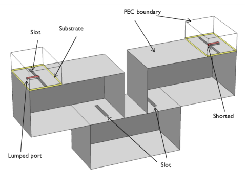
PDF

Cascaded Rectangular Cavity Filter
Introduction
A cascaded cavity filter provides much better bandpass filter performance compared to a single cavity filter. Here, three rectangular cavity filters are coupled via slots and provide excellent out-of-band rejection.
Figure 1: A cascaded rectangular cavity filter consisting of three cavities, coupling slots, and microstrip lines feeds.
Model Definition
The resonant frequencies of a rectangular cavity are given by
where a and b are the dimension of the aperture of a waveguide and d is the length of the waveguide cavity. The size of a single cavity used in this example is 50 mm, 50 mm, 100 mm in depth, height, and width, respectively. The resonant frequency at the dominant mode TE101 is 3.354 GHz. In this example, three such cavities are coupled through slots. The dimensions and locations of the slots can be adjusted to improve input matching properties as well as power transfer between in and output ports. Two shorted microstrip lines, fed by a lumped port, couple into the first and last cavities of the structure. The air box around the microstrip lines is enclosed by metallic walls, representing the packaging.
Results and Discussion
Solving the model over a range of frequencies reveals that the resonant frequency of the cascaded filter is 3.354 GHz, as expected. The out-of-band rejection at ±90 MHz is better than -60 dB.
Figure 2: A plot of the electric field shows the dominant TE101 mode in each cavity.
Figure 3: Frequency response of the cascaded rectangular cavity filter shows good bandpass characteristics.
Notes About the COMSOL Implementation
This example also uses the Frequency Domain Modal study step combined with an Eigenfrequency analysis to evaluate the frequency response of the filter circuit. This approach is faster than a regular frequency sweep performed in a Frequency Domain study, but its usage is limited to only high-Q devices or circuits presenting bandpass frequency properties excited by lumped ports. Since an Eigenfrequency analysis is computationally intensive, it may require more than 8 GB of RAM.
Reference
1. D.M. Pozar, Microwave Engineering, John Wiley & Sons, 1998.
Application Library path: RF_Module/Filters/cascaded_cavity_filter
Modeling Instructions
From the File menu, choose New.
New
In the New window, click  Model Wizard.
Model Wizard
1
In the Model Wizard window, click  3D.
2
In the Select Physics tree, select Radio Frequency>Electromagnetic Waves, Frequency Domain (emw).
3
Click Add.
4
Click  Study.
5
In the Select Study tree, select General Studies>Frequency Domain.
6
Study 1
Step 1: Frequency Domain
1
In the Model Builder window, under Study 1 click Step 1: Frequency Domain.
2
In the Settings window for Frequency Domain, locate the Study Settings section.
3
In the Frequencies text field, type range(3.3[GHz],2.5[MHz],3.38[GHz]).
Global Definitions
Parameters 1
1
In the Model Builder window, under Global Definitions click Parameters 1.
2
In the Settings window for Parameters, locate the Parameters section.
3
Click  Load from File.
4
Here mil refers to the unit milliinch, that is 1 mil = 0.0254 mm.
Geometry 1
1
In the Model Builder window, under Component 1 (comp1) click Geometry 1.
2
In the Settings window for Geometry, locate the Units section.
3
From the Length unit list, choose mm.
Create a cavity at the input port.
Cavity1
1
In the Geometry toolbar, click  Block.
2
In the Settings window for Block, type Cavity1 in the Label text field.
3
Locate the Size and Shape section. In the Width text field, type w_cavity.
4
In the Depth text field, type d_cavity.
5
In the Height text field, type d_cavity.
6
Locate the Position section. From the Base list, choose Center.
7
In the x text field, type -w_cavity/2-w_cavity/8.
8
In the z text field, type d_cavity.
9
Click  Build Selected.
Create a substrate at the input port.
Substrate
1
In the Geometry toolbar, click  Block.
2
In the Settings window for Block, type Substrate in the Label text field.
3
Locate the Size and Shape section. In the Width text field, type w_cavity/3.
4
In the Depth text field, type d_cavity.
5
In the Height text field, type d.
6
Locate the Position section. In the x text field, type -w_cavity-w_cavity/8.
7
In the y text field, type -w_cavity/4.
8
In the z text field, type d_cavity*1.5.
9
Click  Build Selected.
Create a microstrip line at the input port.
Feed
1
In the Geometry toolbar, click  Block.
2
In the Settings window for Block, type Feed in the Label text field.
3
Locate the Size and Shape section. In the Width text field, type l_feed+w_slot.
4
In the Depth text field, type 3.2[mm].
5
In the Height text field, type d.
6
Locate the Position section. From the Base list, choose Center.
7
In the x text field, type -w_cavity/2-w_cavity/8-x_slot-l_feed/2.
8
In the z text field, type d_cavity*1.5+d/2.
9
Click  Build Selected.
To see the interior, you can choose wireframe rendering:
10
Click the  Wireframe Rendering button in the Graphics toolbar.
Create a box enclosing the input port.
FeedBoxBlock
1
In the Geometry toolbar, click  Block.
2
In the Settings window for Block, type FeedBoxBlock in the Label text field.
3
Locate the Size and Shape section. In the Width text field, type w_cavity/3.
4
In the Depth text field, type d_cavity.
5
In the Height text field, type h_feed.
6
Locate the Position section. From the Base list, choose Center.
7
In the x text field, type -w_cavity-w_cavity/8+w_cavity/6.
8
In the z text field, type d_cavity*1.5+h_feed/2.
9
Click  Build Selected.
Create coupling slots between the cavities.
Work Plane 1 (wp1)
1
In the Geometry toolbar, click  Work Plane.
2
In the Settings window for Work Plane, locate the Plane Definition section.
3
In the z-coordinate text field, type 25[mm].
4
Click  Show Work Plane.
Work Plane 1 (wp1)>Rectangle 1 (r1)
1
In the Work Plane toolbar, click  Rectangle.
2
In the Settings window for Rectangle, locate the Size and Shape section.
3
In the Width text field, type 3.5[mm].
4
In the Height text field, type 26.4[mm].
5
Locate the Position section. From the Base list, choose Center.
6
In the xw text field, type -28.5[mm].
7
Click  Build Selected.
Create coupling slots between the microstrip line feed and the cavity linked to the feed as well.
Work Plane 2 (wp2)
1
In the Model Builder window, right-click Geometry 1 and choose Work Plane.
2
In the Settings window for Work Plane, locate the Plane Definition section.
3
In the z-coordinate text field, type 75[mm].
4
Click  Show Work Plane.
Work Plane 2 (wp2)>Rectangle 1 (r1)
1
In the Work Plane toolbar, click  Rectangle.
2
In the Settings window for Rectangle, locate the Size and Shape section.
3
In the Width text field, type w_slot.
4
In the Height text field, type 45[mm].
5
Locate the Position section. From the Base list, choose Center.
6
In the xw text field, type -w_cavity/2-w_cavity/8-x_slot.
7
Right-click Geometry 1 and choose Build All.
Generate the second cavity by mirroring the first one.
Mirror 1 (mir1)
1
In the Geometry toolbar, click  Transforms and choose Mirror.
2
Click in the Graphics window and then press Ctrl+A to select all objects.
3
In the Settings window for Mirror, locate the Normal Vector to Plane of Reflection section.
4
In the x text field, type 1.
5
In the z text field, type 0.
6
Locate the Input section. Select the Keep input objects check box.
7
Click  Build All Objects.
8
Click the  Zoom Extents button in the Graphics toolbar.
Cavity1.1 (blk5)
1
In the Model Builder window, under Component 1 (comp1)>Geometry 1 right-click Cavity1 (blk1) and choose Duplicate.
2
In the Settings window for Block, locate the Position section.
3
In the x text field, type 0.
4
In the z text field, type 0.
5
Click  Build All Objects.
Electromagnetic Waves, Frequency Domain (emw)
The default boundary condition is perfect electric conductor, which is applied to all exterior boundaries. Assign perfect electric conductor to interior boundaries on the cavity walls and microstrip lines.
Perfect Electric Conductor 2
1
In the Model Builder window, under Component 1 (comp1) right-click Electromagnetic Waves, Frequency Domain (emw) and choose the boundary condition Perfect Electric Conductor.
2
Assign a lumped port with port excitation at the end of one microstrip line.
Lumped Port 1
1
In the Physics toolbar, click  Boundaries and choose Lumped Port.
2
For the first port, wave excitation is on by default.
Assign a lumped port at the end of the other microstrip line.
Lumped Port 2
1
In the Physics toolbar, click  Boundaries and choose Lumped Port.
2
Add Material
1
In the Home toolbar, click  Add Material to open the Add Material window.
2
Go to the Add Material window.
3
4
Click Add to Component in the window toolbar.
5
In the Home toolbar, click  Add Material to close the Add Material window.
Materials
Create a dielectric material for the substrates.
Material 2 (mat2)
1
In the Model Builder window, under Component 1 (comp1) right-click Materials and choose Blank Material.
2
3
In the Settings window for Material, locate the Material Contents section.
4
Mesh 1
1
In the Model Builder window, under Component 1 (comp1) click Mesh 1.
2
In the Settings window for Mesh, locate the Physics-Controlled Mesh section.
3
From the Element size list, choose Fine.
4
Click  Build All.
Study 1
In the Home toolbar, click  Compute.
Results
Electric Field (emw)
The default plot shows the norm of the electric field for the highest frequency. Follow the instructions to reproduce Figure 2.
1
In the Settings window for 3D Plot Group, locate the Data section.
2
From the Parameter value (freq (GHz)) list, choose 3.34.
Multislice
1
In the Model Builder window, expand the Electric Field (emw) node, then click Multislice.
2
In the Settings window for Multislice, locate the Multiplane Data section.
3
Find the X-planes subsection. In the Planes text field, type 0.
4
Find the Z-planes subsection. From the Entry method list, choose Coordinates.
5
In the Coordinates text field, type -d_cavity/2+0.1,d_cavity/2+0.1,d_cavity/2*3-0.1.
6
Click to expand the Range section. Select the Manual color range check box.
7
In the Maximum text field, type 800.
8
In the Electric Field (emw) toolbar, click  Plot.
S-parameter (emw)
1
In the Model Builder window, under Results click S-parameter (emw).
2
In the Settings window for 1D Plot Group, locate the Legend section.
3
From the Position list, choose Lower right.
Smith Plot (emw)
3D Plot Group 4
1
In the Home toolbar, click  Add Plot Group and choose 3D Plot Group.
2
In the Settings window for 3D Plot Group, locate the Data section.
3
From the Parameter value (freq (GHz)) list, choose 3.34.
Isosurface 1
1
Right-click 3D Plot Group 4 and choose Isosurface.
2
In the Settings window for Isosurface, locate the Levels section.
3
In the Total levels text field, type 20.
4
Locate the Coloring and Style section. Click  Change Color Table.
5
In the Color Table dialog box, select Aurora>AuroraBorealis in the tree.
6
Filter 1
1
Right-click Isosurface 1 and choose Filter.
2
In the Settings window for Filter, locate the Element Selection section.
3
In the Logical expression for inclusion text field, type y>0.
4
In the 3D Plot Group 4 toolbar, click  Plot.
Analyze the same model with a Frequency Domain Modal method. When a device presents resonances, the Frequency Domain Modal method combined with an Eigenfrequency analysis provides a faster solution time.
Electromagnetic Waves, Frequency Domain (emw)
Lumped Port 1
1
In the Model Builder window, under Component 1 (comp1)>Electromagnetic Waves, Frequency Domain (emw) click Lumped Port 1.
2
In the Settings window for Lumped Port, locate the Boundary Selection section.
3
Click  Create Selection.
4
In the Create Selection dialog box, Create a set of selections for use in the study settings.
5
type Lumped port 1 in the Selection name text field.
6
Lumped Port 2
1
In the Model Builder window, click Lumped Port 2.
2
In the Settings window for Lumped Port, locate the Boundary Selection section.
3
Click  Create Selection.
4
In the Create Selection dialog box, type Lumped port 2 in the Selection name text field.
5
Add Study
1
In the Home toolbar, click  Add Study to open the Add Study window.
2
Go to the Add Study window.
3
Find the Studies subsection. In the Select Study tree, select Preset Studies for Selected Physics Interfaces>Frequency Domain, Modal.
4
Click Add Study in the window toolbar.
5
In the Home toolbar, click  Add Study to close the Add Study window.
Study 2
Step 1: Eigenfrequency
1
In the Settings window for Eigenfrequency, locate the Study Settings section.
2
In the Search for eigenfrequencies around text field, type 3.3[GHz].
Step 2: Frequency Domain, Modal
1
In the Model Builder window, click Step 2: Frequency Domain, Modal.
2
In the Settings window for Frequency Domain, Modal, locate the Study Settings section.
3
In the Frequencies text field, type range(3.3[GHz],2.5[MHz]/50,3.38[GHz]).
With a 50 times finer frequency step, the solutions will increase the file size tremendously when it is saved. When only S-parameters are of interest, a common theme in most passive RF and microwave device designs, it is not necessary to store all of the field solutions. By selecting the Store fields in output check box in the Values of Dependent Variables section, we can control the part of the model on which the computed solution is saved. We only add the selection containing these boundaries where the S-parameters are calculated. The lumped port size is typically very small compared to the entire modeling domain, and the saved file size with the finer frequency step is more or less that of the regular discrete frequency sweep model when only the solutions on the port boundaries are stored.
4
Click to expand the Values of Dependent Variables section. Find the Store fields in output subsection. From the Settings list, choose For selections.
5
Under Selections, click  Add.
6
In the Add dialog box, in the Selections list, choose Lumped port 1 and Lumped port 2.
7
8
In the Home toolbar, click  Compute.
Results
Electric Field (emw) 1
Since the results are stored only on the lumped port boundaries, this default E-field norm plot does not provide useful information.
1
Right-click Results>Electric Field (emw) 1 and choose Delete.
Generate all S-parameters from each analysis on the same plot and compare them to each other.
S-parameter (emw) 1
1
In the Model Builder window, under Results click S-parameter (emw) 1.
2
In the Settings window for 1D Plot Group, click to expand the Title section.
3
From the Title type list, choose Manual.
4
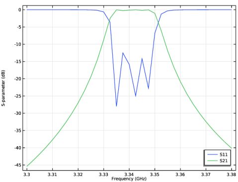
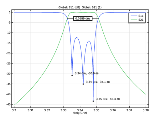
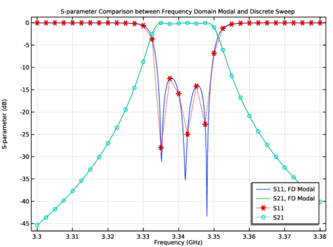
In the Title text area, type S-parameter Comparison between Frequency Domain Modal and Discrete Sweep.
5
Locate the Legend section. From the Position list, choose Lower right.
Global 2
1
In the Model Builder window, expand the S-parameter (emw) 1 node.
2
Right-click Results>S-parameter (emw) 1>Global 1 and choose Duplicate.
3
In the Settings window for Global, locate the Data section.
4
From the Dataset list, choose Study 1/Solution 1 (sol1).
5
Click to expand the Coloring and Style section. Find the Line style subsection. From the Line list, choose Dotted.
6
Find the Line markers subsection. From the Marker list, choose Cycle.
Global 1
1
In the Model Builder window, click Global 1.
2
In the Settings window for Global, locate the y-Axis Data section.
3
4
In the S-parameter (emw) 1 toolbar, click  Plot.
See Figure 3 for S-parameter plot.
Smith Plot (emw) 1
Compare the solution time between two studies.
The following instruction shows how to use the Graph Marker subfeature to analyze 1D plots. When plotting S11 of a bandpass filter, poles are of interest and a graph marker captures the local minima. For analyzing the insertion loss such as S21, the -3dB bandwidth of the passband can be computed through an additional graph marker.
S-parameter with Graph Markers
1
In the Home toolbar, click  Add Plot Group and choose 1D Plot Group.
2
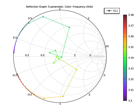
In the Settings window for 1D Plot Group, type S-parameter with Graph Markers in the Label text field.
3
Locate the Data section. From the Dataset list, choose Study 2/Solution 2 (sol2).
Global 1
1
Right-click S-parameter with Graph Markers and choose Global.
2
In the Settings window for Global, click Add Expression in the upper-right corner of the y-Axis Data section. From the menu, choose Component 1 (comp1)>Electromagnetic Waves, Frequency Domain>Ports>S-parameter, dB>emw.S11dB - S11.
3
Locate the y-Axis Data section. In the table, enter the following settings:
Graph Marker 1
1
Right-click Global 1 and choose Graph Marker.
2
In the Settings window for Graph Marker, locate the Display section.
3
From the Display list, choose Min.
4
From the Scope list, choose Local.
5
Locate the Text Format section. In the Display precision text field, type 3.
6
Select the Show x-coordinate check box.
7
Select the Include unit check box.
8
Click to expand the Coloring and Style section. From the Anchor point list, choose Lower left.
Global 2
1
In the Model Builder window, right-click S-parameter with Graph Markers and choose Global.
2
In the Settings window for Global, click Replace Expression in the upper-right corner of the y-Axis Data section. From the menu, choose Component 1 (comp1)>Electromagnetic Waves, Frequency Domain>Ports>S-parameter, dB>emw.S21dB - S21.
Graph Marker 1
1
Right-click Global 2 and choose Graph Marker.
2
In the Settings window for Graph Marker, locate the Display section.
3
From the Display mode list, choose Bandwidth.
4
Locate the Text Format section. In the Display precision text field, type 3.
5
Select the Include unit check box.
6
Locate the Coloring and Style section. Select the Show frame check box.