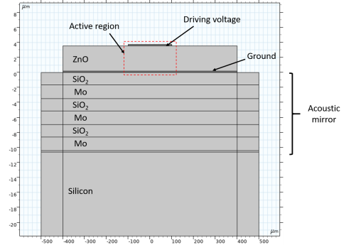
PDF

Solidly Mounted Resonator 3D
Introduction
A solidly mounted resonator (SMR) is a piezoelectric MEMS resonator formed on top of an acoustic mirror stack deposited on a thick substrate. This tutorial shows how to simulate an SMR in 3D. In this example, the eigenmodes were computed with varying number of particles attached to the sensor surface for computing the sensitivity, and the corresponding change in frequency response was analyzed. The resonant frequency decreases with more attached particles, and the sensitivity depends on the attachment location relative to the mode shape — both observations are as expected.
Model Definition
The 2D geometry of the SMR model and its key components are shown in Figure 1.
Figure 1: 2D model geometry showing the key components of the solidly mounted resonator.
Note that for clarity, the vertical scale is magnified to show the layers.
In the 3D model, to save computation resources, symmetry planes are used to reduce the modeling domain to 1/4 of the full device as shown in Figure 2. All dimensions are parameterized in the model. Various selection features are used for the construction of the geometry and the setup of physics and mesh.
Figure 2: Model geometry.
The fabrication of the device is discussed in Ref. 1. Here we provide a description of the final structure and an explanation of its principle of operation.
At the top of the device is a ZnO piezoelectric layer with aluminum electrodes at its top (drive) and bottom (ground) surfaces. Here, the pole direction is along the vertical axis and the piezoelectric material data is available in the built-in MEMS material library.
Underneath the piezoelectric resonator is a stack of alternating layers of molybdenum (high impedance) and silicon dioxide (low impedance). The thickness of the molybdenum and silicon dioxide layers were chosen to be 1.82 µm and 1.65 µm, respectively, to reflect the acoustic wave generated by the piezoelectric resonator and to prevent its dissipation in the silicon substrate. With this structure, the resonant frequency of the device is 870 MHz.
The parameters of the geometry are summarized in the first table in the section Modeling Instructions. The second table in the same section summarizes the material properties used in the model as specified in Ref. 1. Other material properties used in the model are obtained from the MEMS Module material library. As shown in the table, the Young’s moduli of the materials and the wavelength in silicon are computed from the values of density and acoustic velocity listed in the paper.
In this model, the fully coupled structural and electrostatic equations are solved in the piezoelectric layer, while only the structural equation is solved in other layers. Electrostatics equations are not solved in the aluminum layers because of its high electrical conductivity.
Perfectly Matching Layers (PML) boundary conditions are used at the sides and the bottom of the device to introduce anchor damping and eliminate reflections. The model also includes mechanical losses through an isotropic structural loss factor of 1.5 × 10-4. The model has fixed boundary conditions at the outer edges of the PML.
In addition to the device structure, six cubes of 1 um size are added to the geometry to represent particles attached to the active area of the sensor (Figure 3). The global parameters p1 ~ p6 are used to switch on/off the particles by scaling the material density.
Figure 3: Six cubes of 1 um size to model attached particles.
The effect of the particles are investigated using Eigenfrequency and Frequency Domain studies.
To save time and reduce file size, a relatively coarse mesh is used, in particular in the horizontal direction. Thus only the main lower modes will be resolved in this model. The same approach was taken in the reference paper.
Figure 4: The mesh used in the model.
Results and Discussion
Figure 5 shows the mode shape of the fundamental mode of the resonator with the resonant frequency of about 870 MHz as intended by the design described in Ref. 1.
Figure 5: Mode shape of the resonator’s fundamental mode.
In the next two figures, the same mode shape is plotted with two particles attached to the sensor surface. It will be seen that both the mode shape variation and the frequency shift depend on the location of the particles.
Figure 6 shows the mode shape with two particles attached at the periphery of the sensor. The frequency shift is small and the mode shape does not change much.
Figure 6: Mode shape with two particles attached at the periphery.
Figure 7 shows the mode shape with two particles attached close to the center of the sensor. The frequency shift is large and the mode shape is perturbed significantly.
Figure 7: Mode shape with two particles attached close to the center.
The fact that the response of the sensor to attached particles depends on the particle locations is further illustrated in the plot of resonant frequency versus total particle mass below. The scatter of the data points demonstrates the dependence on the particle locations. The sensitivity is estimated to be about 10 MHz/ng from the graph.
Figure 8: Resonant frequency versus total particle mass.
Figure 9 plots the electric potential at resonance from the frequency domain study.
Figure 9: Electric potential at resonance.
Figure 10 shows the expected trend of lower resonant frequency with attached particles.
Figure 10: Frequency response with versus without attached particles.
Reference
1. F.H. Villa-López and others, “Design and Modelling of Solidly Mounted Resonators for Low-Cost Particle Sensing,” Measurement Science and Technology, vol. 27, no. 2, 2016.
Application Library path: MEMS_Module/Piezoelectric_Devices/solidly_mounted_resonator_3d
Modeling Instructions
Start with a new 3D model with the built-in piezoelectric physics.
From the File menu, choose New.
New
In the New window, click  Model Wizard.
Model Wizard
1
In the Model Wizard window, click  3D.
2
In the Select Physics tree, select Structural Mechanics>Electromagnetics-Structure Interaction>Piezoelectricity>Piezoelectricity, Solid.
3
Click Add.
4
Click  Study.
5
In the Select Study tree, select Preset Studies for Selected Multiphysics>Eigenfrequency.
6
Geometry 1
Set the geometry unit to microns for convenience.
1
In the Model Builder window, under Component 1 (comp1) click Geometry 1.
2
In the Settings window for Geometry, locate the Units section.
3
From the Length unit list, choose µm.
Enter geometry parameters. Note that we will truncate most of the thickness of the Si substrate and replace it with a perfectly matched layer (PML).
Global Definitions
Parameters 1 - Geometry
1
In the Model Builder window, under Global Definitions click Parameters 1.
2
In the Settings window for Parameters, type Parameters 1 - Geometry in the Label text field.
3
Locate the Parameters section. In the table, enter the following settings:
Enter material parameters. Then calculate the Young’s Modulus from the density and acoustic velocity for each linear material. Also calculate the wavelength in the substrate for an estimate of the PML thickness. A guessed value of 1.5e-4 is used for an isotropic damping factor as in the case of the 2D model. The parameters p1 ~ p6 will be used to switch on/off each of the 6 particles attached to the active area of the sensor by scaling the material density.
Parameters 2 - Material properties
1
In the Home toolbar, click  Parameters and choose Add>Parameters.
2
In the Settings window for Parameters, type Parameters 2 - Material properties in the Label text field.
3
Locate the Parameters section. In the table, enter the following settings:
Build the parameterized geometry. Only 1/4 of the geometry will be built due to symmetry. Note how the selection and cumulative selection functionalities will be used to created named selections for material and physics settings later.
Geometry 1
Piezo - ZnO
1
In the Geometry toolbar, click  Block.
2
In the Settings window for Block, type Piezo - ZnO in the Label text field.
3
Locate the Size and Shape section. In the Width text field, type w_pe/2.
4
In the Depth text field, type w_pe/2.
5
In the Height text field, type t_pe.
6
Locate the Selections of Resulting Entities section. Select the Resulting objects selection check box.
Bottom electrode
1
Right-click Piezo - ZnO and choose Duplicate.
2
In the Settings window for Block, type Bottom electrode in the Label text field.
3
Locate the Size and Shape section. In the Height text field, type t_e.
4
Locate the Position section. In the z text field, type -t_e.
5
Locate the Selections of Resulting Entities section. From the Show in physics list, choose All levels.
6
Find the Cumulative selection subsection. Click New.
7
In the New Cumulative Selection dialog box, type Al in the Name text field.
8
Top electrode
1
Right-click Bottom electrode and choose Duplicate.
2
In the Settings window for Block, type Top electrode in the Label text field.
3
Locate the Size and Shape section. In the Width text field, type w_ar/2.
4
In the Depth text field, type w_ar/2.
5
Locate the Position section. In the z text field, type t_pe.
Low impedance - SiO2
1
In the Geometry toolbar, click  Block.
2
In the Settings window for Block, type Low impedance - SiO2 in the Label text field.
3
Locate the Size and Shape section. In the Width text field, type w/2.
4
In the Depth text field, type w/2.
5
In the Height text field, type t_lil.
6
Locate the Position section. In the z text field, type -t_lil-t_e.
7
Click to expand the Layers section. In the table, enter the following settings:
8
Find the Layer position subsection. Select the Right check box.
9
Select the Back check box.
10
Clear the Bottom check box.
11
Locate the Selections of Resulting Entities section. Find the Cumulative selection subsection. Click New.
12
In the New Cumulative Selection dialog box, type SiO2 in the Name text field.
13
Array - SiO2
1
In the Geometry toolbar, click  Transforms and choose Array.
2
In the Settings window for Array, type Array - SiO2 in the Label text field.
3
Locate the Selections of Resulting Entities section. Select the Resulting objects selection check box.
4
Locate the Input section. From the Input objects list, choose SiO2.
5
Locate the Size section. In the z size text field, type 3.
6
Locate the Displacement section. In the z text field, type -t_lil-t_hil.
High impedance - Mo
1
In the Model Builder window, under Component 1 (comp1)>Geometry 1 right-click Low impedance - SiO2 (blk4) and choose Duplicate.
2
In the Settings window for Block, type High impedance - Mo in the Label text field.
3
Locate the Size and Shape section. In the Height text field, type t_hil.
4
Locate the Position section. In the z text field, type -t_hil-t_lil-t_e.
5
Locate the Selections of Resulting Entities section. Find the Cumulative selection subsection. Click New.
6
In the New Cumulative Selection dialog box, type Mo in the Name text field.
7
Array - Mo
1
In the Model Builder window, under Component 1 (comp1)>Geometry 1 right-click Array - SiO2 (arr1) and choose Duplicate.
2
In the Settings window for Array, type Array - Mo in the Label text field.
3
Locate the Input section. Find the Input objects subsection. Click to select the  Activate Selection toggle button.
4
From the Input objects list, choose Mo.
5
Click  Build Selected.
Insulator - SiO2
1
In the Model Builder window, under Component 1 (comp1)>Geometry 1 right-click Low impedance - SiO2 (blk4) and choose Duplicate.
2
In the Settings window for Block, type Insulator - SiO2 in the Label text field.
3
Locate the Size and Shape section. In the Height text field, type t_i.
4
Locate the Position section. In the z text field, type -3*t_hil-3*t_lil-t_e-t_i.
Substrate - Si
1
Right-click Insulator - SiO2 and choose Duplicate.
2
In the Settings window for Block, type Substrate - Si in the Label text field.
3
Locate the Size and Shape section. In the Height text field, type t_s.
4
Locate the Position section. In the z text field, type -3*t_hil-3*t_lil-t_e-t_i-t_s.
5
Locate the Selections of Resulting Entities section. Select the Resulting objects selection check box.
6
Find the Cumulative selection subsection. Click New.
7
In the New Cumulative Selection dialog box, type Si in the Name text field.
8
Bottom PML - Si
1
Right-click Substrate - Si and choose Duplicate.
2
In the Settings window for Block, type Bottom PML - Si in the Label text field.
3
Locate the Size and Shape section. In the Height text field, type lambda_Si.
4
Locate the Position section. In the z text field, type -3*t_hil-3*t_lil-t_e-t_i-t_s-lambda_Si.
Add 6 blocks at arbitrarily chosen locations on top of the active area to represent particles of 1 micron size attached to the sensor. These will be activated or deactivated using the parameters p1 ~ p6 as described earlier.
Particle 1
1
In the Geometry toolbar, click  Block.
2
In the Settings window for Block, type Particle 1 in the Label text field.
3
Locate the Position section. In the x text field, type 15.
4
In the y text field, type 25.
5
In the z text field, type t_pe+t_e.
6
Locate the Selections of Resulting Entities section. Select the Resulting objects selection check box.
7
Find the Cumulative selection subsection. Click New.
8
In the New Cumulative Selection dialog box, type Particles in the Name text field.
9
Particle 2
1
Right-click Particle 1 and choose Duplicate.
2
In the Settings window for Block, type Particle 2 in the Label text field.
3
Locate the Position section. In the x text field, type 50.
4
In the y text field, type 15.
Particle 3
1
Right-click Particle 2 and choose Duplicate.
2
In the Settings window for Block, type Particle 3 in the Label text field.
3
Locate the Position section. In the x text field, type 39.
4
In the y text field, type 51.
Particle 4
1
Right-click Particle 3 and choose Duplicate.
2
In the Settings window for Block, type Particle 4 in the Label text field.
3
Locate the Position section. In the x text field, type 55.
4
In the y text field, type 35.
Particle 5
1
Right-click Particle 4 and choose Duplicate.
2
In the Settings window for Block, type Particle 5 in the Label text field.
3
Locate the Position section. In the x text field, type 62.
4
In the y text field, type 80.
Particle 6
1
Right-click Particle 5 and choose Duplicate.
2
In the Settings window for Block, type Particle 6 in the Label text field.
3
Locate the Position section. In the x text field, type 85.
4
In the y text field, type 55.
5
In the Geometry toolbar, click  Build All.
Create selections for the PML, symmetry boundary condition, fixed boundary condition, the top surfaces of the particles, and the acoustic mirror. Use wireframe rendering to more easily see the defined selections.
Definitions
Symmetry BC 1
1
In the Definitions toolbar, click  Box.
2
In the Settings window for Box, type Symmetry BC 1 in the Label text field.
3
Locate the Geometric Entity Level section. From the Level list, choose Boundary.
4
Locate the Box Limits section. In the x maximum text field, type eps.
5
Locate the Output Entities section. From the Include entity if list, choose Entity inside box.
6
Click the  Wireframe Rendering button in the Graphics toolbar.
Symmetry BC 2
1
Right-click Symmetry BC 1 and choose Duplicate.
2
In the Settings window for Box, type Symmetry BC 2 in the Label text field.
3
Locate the Box Limits section. In the x maximum text field, type Inf.
4
In the y maximum text field, type eps.
Fixed BC bottom
1
Right-click Symmetry BC 2 and choose Duplicate.
2
In the Settings window for Box, type Fixed BC bottom in the Label text field.
3
Locate the Box Limits section. In the y maximum text field, type Inf.
4
In the z maximum text field, type -3*t_hil-3*t_lil-t_e-t_i-t_s-lambda_Si/2.
Fixed BC side 1
1
Right-click Fixed BC bottom and choose Duplicate.
2
In the Settings window for Box, type Fixed BC side 1 in the Label text field.
3
Locate the Box Limits section. In the x minimum text field, type (w/2+w_pe/2)/2.
4
In the z maximum text field, type Inf.
Fixed BC side 2
1
Right-click Fixed BC side 1 and choose Duplicate.
2
In the Settings window for Box, type Fixed BC side 2 in the Label text field.
3
Locate the Box Limits section. In the x minimum text field, type -Inf.
4
In the y minimum text field, type (w/2+w_pe/2)/2.
Fixed BC
1
In the Definitions toolbar, click  Union.
2
In the Settings window for Union, type Fixed BC in the Label text field.
3
Locate the Geometric Entity Level section. From the Level list, choose Boundary.
4
Locate the Input Entities section. Under Selections to add, click  Add.
5
In the Add dialog box, in the Selections to add list, choose Fixed BC bottom, Fixed BC side 1, and Fixed BC side 2.
6
Not PML
1
In the Definitions toolbar, click  Box.
2
In the Settings window for Box, type Not PML in the Label text field.
3
Locate the Box Limits section. In the x maximum text field, type (w/2+w_pe/2)/2.
4
In the y maximum text field, type (w/2+w_pe/2)/2.
5
In the z minimum text field, type -3*t_hil-3*t_lil-t_e-t_i-t_s-lambda_Si/2.
6
Locate the Output Entities section. From the Include entity if list, choose Entity inside box.
PML
1
In the Definitions toolbar, click  Complement.
2
In the Settings window for Complement, type PML in the Label text field.
3
Locate the Input Entities section. Under Selections to invert, click  Add.
4
In the Add dialog box, select Not PML in the Selections to invert list.
5
Top surfaces of particles
1
In the Model Builder window, right-click Fixed BC bottom and choose Duplicate.
2
In the Settings window for Box, type Top surfaces of particles in the Label text field.
3
Locate the Box Limits section. In the z minimum text field, type t_pe+t_e+1/2.
4
In the z maximum text field, type Inf.
Acoustic mirror
1
In the Definitions toolbar, click  Union.
2
In the Settings window for Union, type Acoustic mirror in the Label text field.
3
Locate the Input Entities section. Under Selections to add, click  Add.
4
In the Add dialog box, in the Selections to add list, choose Mo and Array - SiO2.
5
Create an integration operator over the particle domains to compute the attached particle mass.
Integration - Particles
1
In the Definitions toolbar, click  Nonlocal Couplings and choose Integration.
2
In the Settings window for Integration, type Integration - Particles in the Label text field.
3
Locate the Source Selection section. From the Selection list, choose Particles.
Create the Perfectly Matched Layers.
Perfectly Matched Layer 1 (pml1)
1
In the Definitions toolbar, click  Perfectly Matched Layer.
2
In the Settings window for Perfectly Matched Layer, locate the Domain Selection section.
3
From the Selection list, choose PML.
Before adding material properties, set up the physics settings, so that the required properties will be highlighted when adding materials. Use the selections made earlier for the physics selections. For Solid Mechanics: add damping subnodes, symmetry boundary conditions, and fixed boundary conditions.
Solid Mechanics (solid)
Linear Elastic Material 1
In the Model Builder window, under Component 1 (comp1)>Solid Mechanics (solid) click Linear Elastic Material 1.
Damping 1
1
In the Physics toolbar, click  Attributes and choose Damping.
2
In the Settings window for Damping, locate the Damping Settings section.
3
From the Damping type list, choose Isotropic loss factor.
Piezoelectric Material 1
1
In the Model Builder window, under Component 1 (comp1)>Solid Mechanics (solid) click Piezoelectric Material 1.
2
In the Settings window for Piezoelectric Material, locate the Domain Selection section.
3
From the Selection list, choose Piezo - ZnO.
Mechanical Damping 1
In the Physics toolbar, click  Attributes and choose Mechanical Damping.
Fixed Constraint 1
1
In the Physics toolbar, click  Boundaries and choose Fixed Constraint.
2
In the Settings window for Fixed Constraint, locate the Boundary Selection section.
3
From the Selection list, choose Fixed BC.
Symmetry 1
1
In the Physics toolbar, click  Boundaries and choose Symmetry.
2
In the Settings window for Symmetry, locate the Boundary Selection section.
3
From the Selection list, choose Symmetry BC 1.
Symmetry 2
1
In the Physics toolbar, click  Boundaries and choose Symmetry.
2
In the Settings window for Symmetry, locate the Boundary Selection section.
3
From the Selection list, choose Symmetry BC 2.
For Electrostatics: only the domain surrounded by electrodes (the piezo domain) needs to be selected. Use the Terminal boundary condition (not the Electric Potential boundary condition) for the excitation port, so that lumped electrical parameters will be computed automatically. Drive the terminal with a voltage of 1 V.
Electrostatics (es)
1
In the Model Builder window, under Component 1 (comp1) click Electrostatics (es).
2
In the Settings window for Electrostatics, locate the Domain Selection section.
3
From the Selection list, choose Piezo - ZnO.
Ground 1
1
In the Physics toolbar, click  Boundaries and choose Ground.
2
In the Settings window for Ground, locate the Boundary Selection section.
3
From the Selection list, choose Bottom electrode.
Terminal 1
1
In the Physics toolbar, click  Boundaries and choose Terminal.
2
In the Settings window for Terminal, locate the Boundary Selection section.
3
From the Selection list, choose Top electrode.
4
Locate the Terminal section. From the Terminal type list, choose Voltage.
The domain and physics selections of the Piezoelectric Effect multiphysics coupling should be set up automatically.
Multiphysics
Piezoelectric Effect 1 (pze1)
Add material properties from the COMSOL Piezoelectric, MEMS, and Built-in material folders as an initial template. Then enter the available data from the reference paper using the parameters prepared earlier under Parameters 2 - Material properties.
Add Material
1
In the Home toolbar, click  Add Material to open the Add Material window.
2
Go to the Add Material window.
3
In the tree, select Piezoelectric>Zinc Oxide.
4
Click Add to Component in the window toolbar.
Materials
Zinc Oxide (mat1)
1
In the Settings window for Material, locate the Geometric Entity Selection section.
2
From the Selection list, choose Piezo - ZnO.
3
Locate the Material Contents section. In the table, enter the following settings:
Add Material
1
Go to the Add Material window.
2
In the tree, select MEMS>Metals>Al - Aluminum.
3
Click Add to Component in the window toolbar.
Materials
Al - Aluminum (mat2)
1
In the Settings window for Material, locate the Geometric Entity Selection section.
2
From the Selection list, choose Al.
3
Locate the Material Contents section. In the table, enter the following settings:
Add Material
1
Go to the Add Material window.
2
In the tree, select MEMS>Insulators>SiO2 - Silicon oxide.
3
Click Add to Component in the window toolbar.
Materials
SiO2 - Silicon oxide (mat3)
1
In the Settings window for Material, locate the Geometric Entity Selection section.
2
From the Selection list, choose SiO2.
3
Locate the Material Contents section. In the table, enter the following settings:
Add Material
1
Go to the Add Material window.
2
In the tree, select MEMS>Semiconductors>Si - Silicon (single-crystal, isotropic).
3
Click Add to Component in the window toolbar.
Materials
Si - Silicon (single-crystal, isotropic) (mat4)
1
In the Settings window for Material, locate the Geometric Entity Selection section.
2
From the Selection list, choose Si.
3
Locate the Material Contents section. In the table, enter the following settings:
Add Material
1
Go to the Add Material window.
2
In the tree, select Built-in>Molybdenum.
3
Click Add to Component in the window toolbar.
4
In the Home toolbar, click  Add Material to close the Add Material window.
Materials
Molybdenum (mat5)
1
In the Settings window for Material, locate the Geometric Entity Selection section.
2
From the Selection list, choose Mo.
3
Locate the Material Contents section. In the table, enter the following settings:
For the particle material, duplicated the SiO2 material node and define a variable p for each particle domain using the corresponding parameters p1 ~ p6 to scale the density of each particle accordingly (as a way to switch each particle on and off).
Definitions
Variables - Particle 1
1
In the Model Builder window, under Component 1 (comp1) right-click Definitions and choose Variables.
2
In the Settings window for Variables, type Variables - Particle 1 in the Label text field.
3
Locate the Geometric Entity Selection section. From the Geometric entity level list, choose Domain.
4
From the Selection list, choose Particle 1.
5
Locate the Variables section. In the table, enter the following settings:
Variables - Particle 2
1
Right-click Variables - Particle 1 and choose Duplicate.
2
In the Settings window for Variables, type Variables - Particle 2 in the Label text field.
3
Locate the Geometric Entity Selection section. From the Selection list, choose Particle 2.
4
Locate the Variables section. In the table, enter the following settings:
Variables - Particle 3
1
Right-click Variables - Particle 2 and choose Duplicate.
2
In the Settings window for Variables, type Variables - Particle 3 in the Label text field.
3
Locate the Geometric Entity Selection section. From the Selection list, choose Particle 3.
4
Locate the Variables section. In the table, enter the following settings:
Variables - Particle 4
1
Right-click Variables - Particle 3 and choose Duplicate.
2
In the Settings window for Variables, type Variables - Particle 4 in the Label text field.
3
Locate the Geometric Entity Selection section. From the Selection list, choose Particle 4.
4
Locate the Variables section. In the table, enter the following settings:
Variables - Particle 5
1
Right-click Variables - Particle 4 and choose Duplicate.
2
In the Settings window for Variables, type Variables - Particle 5 in the Label text field.
3
Locate the Geometric Entity Selection section. From the Selection list, choose Particle 5.
4
Locate the Variables section. In the table, enter the following settings:
Variables - Particle 6
1
Right-click Variables - Particle 5 and choose Duplicate.
2
In the Settings window for Variables, type Variables - Particle 6 in the Label text field.
3
Locate the Geometric Entity Selection section. From the Selection list, choose Particle 6.
4
Locate the Variables section. In the table, enter the following settings:
Materials
SiO2 Particles
1
In the Model Builder window, under Component 1 (comp1)>Materials right-click SiO2 - Silicon oxide (mat3) and choose Duplicate.
2
In the Settings window for Material, type SiO2 Particles in the Label text field.
3
Locate the Geometric Entity Selection section. From the Selection list, choose Particles.
4
Locate the Material Contents section. In the table, enter the following settings:
5
Click the  Zoom to Selection button in the Graphics toolbar.
To save time and file size, a relatively coarse mesh will be used, in particular in the horizontal direction. Thus only the main lower modes will be resolved in this model. The same approach was taken in the reference paper. The general approach in the following meshing procedure is: Starting from the top surfaces, build triangular mesh on the surfaces and then sweep downwards, except for the PMLs, which should use mapped mesh and then sweep downwards.
Mesh 1
Free Triangular - Top surfaces of particles
1
In the Mesh toolbar, click  Boundary and choose Free Triangular.
2
In the Settings window for Free Triangular, type Free Triangular - Top surfaces of particles in the Label text field.
3
Locate the Boundary Selection section. From the Selection list, choose Top surfaces of particles.
Swept - Particles
1
In the Mesh toolbar, click  Swept.
2
In the Settings window for Swept, type Swept - Particles in the Label text field.
3
Locate the Domain Selection section. From the Geometric entity level list, choose Domain.
4
From the Selection list, choose Particles.
Distribution 1
1
Right-click Swept - Particles and choose Distribution.
2
In the Settings window for Distribution, locate the Distribution section.
3
In the Number of elements text field, type 3.
Free Triangular - Top electrode
1
In the Mesh toolbar, click  Boundary and choose Free Triangular.
2
In the Settings window for Free Triangular, type Free Triangular - Top electrode in the Label text field.
3
Size 1
1
Right-click Free Triangular - Top electrode and choose Size.
2
In the Settings window for Size, locate the Element Size section.
3
Click the Custom button.
4
Locate the Element Size Parameters section.
5
Select the Maximum element size check box. In the associated text field, type 10.
6
Select the Minimum element size check box. In the associated text field, type 1.
Swept - Top electrode
1
In the Mesh toolbar, click  Swept.
2
In the Settings window for Swept, type Swept - Top electrode in the Label text field.
3
Locate the Domain Selection section. From the Geometric entity level list, choose Domain.
4
From the Selection list, choose Top electrode.
5
Click  Build All.
6
Click the  Zoom to Selection button in the Graphics toolbar.
Free Triangular - Piezo
1
In the Mesh toolbar, click  Boundary and choose Free Triangular.
2
In the Settings window for Free Triangular, type Free Triangular - Piezo in the Label text field.
3
Swept - Piezo
1
In the Mesh toolbar, click  Swept.
2
In the Settings window for Swept, type Swept - Piezo in the Label text field.
3
Locate the Domain Selection section. From the Geometric entity level list, choose Domain.
4
From the Selection list, choose Piezo - ZnO.
Distribution 1
1
Right-click Swept - Piezo and choose Distribution.
2
In the Settings window for Distribution, locate the Distribution section.
3
In the Number of elements text field, type 6.
Swept - Bottom electrode
1
In the Mesh toolbar, click  Swept.
2
In the Settings window for Swept, type Swept - Bottom electrode in the Label text field.
3
Locate the Domain Selection section. From the Geometric entity level list, choose Domain.
4
From the Selection list, choose Bottom electrode.
5
Click  Build All.
6
Click the  Zoom to Selection button in the Graphics toolbar.
Mapped - PML
1
In the Mesh toolbar, click  Boundary and choose Mapped.
2
In the Settings window for Mapped, type Mapped - PML in the Label text field.
3
4
Click to expand the Reduce Element Skewness section. Select the Adjust edge mesh check box.
Distribution 1
1
Right-click Mapped - PML and choose Distribution.
2
3
In the Settings window for Distribution, locate the Distribution section.
4
In the Number of elements text field, type 3.
Swept - Acoustic mirror
1
In the Mesh toolbar, click  Swept.
2
In the Settings window for Swept, type Swept - Acoustic mirror in the Label text field.
3
Locate the Domain Selection section. From the Geometric entity level list, choose Domain.
4
From the Selection list, choose Acoustic mirror.
Distribution 1
1
Right-click Swept - Acoustic mirror and choose Distribution.
2
In the Settings window for Distribution, locate the Distribution section.
3
In the Number of elements text field, type 3.
Swept - Remaining
1
In the Mesh toolbar, click  Swept.
2
In the Settings window for Swept, type Swept - Remaining in the Label text field.
Distribution - Substrate
1
Right-click Swept - Remaining and choose Distribution.
2
In the Settings window for Distribution, type Distribution - Substrate in the Label text field.
3
Locate the Domain Selection section. Click  Clear Selection.
4
From the Selection list, choose Substrate - Si.
5
Locate the Distribution section. From the Distribution type list, choose Predefined.
6
In the Number of elements text field, type 12.
7
In the Element ratio text field, type 5.
Distribution - PML
1
In the Model Builder window, right-click Swept - Remaining and choose Distribution.
2
In the Settings window for Distribution, type Distribution - PML in the Label text field.
3
Locate the Domain Selection section. Click  Clear Selection.
4
5
Locate the Distribution section. In the Number of elements text field, type 3.
6
Click  Build All.
7
Click the  Zoom Extents button in the Graphics toolbar.
Use the eigenfrequency study to look for the fundamental mode around 870 MHz for a series of specified particles using the Auxiliary sweep.
Study 1 - Eigenfrequency & Sensitivity
1
In the Model Builder window, click Study 1.
2
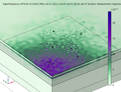
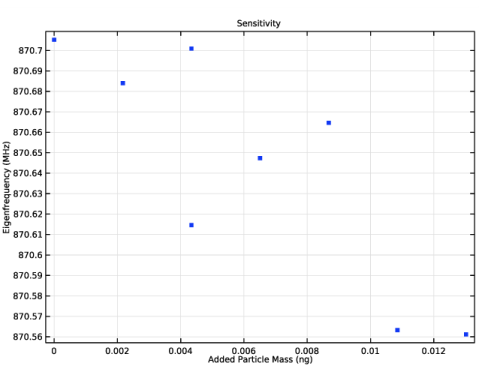
In the Settings window for Study, type Study 1 - Eigenfrequency & Sensitivity in the Label text field.
Step 1: Eigenfrequency
1
In the Model Builder window, under Study 1 - Eigenfrequency & Sensitivity click Step 1: Eigenfrequency.
2
In the Settings window for Eigenfrequency, locate the Study Settings section.
3
Select the Desired number of eigenfrequencies check box. In the associated text field, type 1.
4
Find the Search region subsection. From the Unit list, choose MHz.
5
In the Search for eigenfrequencies around text field, type 870.6.
6
Click to expand the Study Extensions section. Select the Auxiliary sweep check box.
7
8
9
10
11
12
13
14
15
16
17
18
19
In the Home toolbar, click  Compute.
Results
Mode Shape (solid)
Define a selection to exclude the particle surfaces from the mode shape plot. Zoom in to the active region of the sensor to observe the mode shape.
Definitions
Not particles
1
In the Definitions toolbar, click  Complement.
2
In the Settings window for Complement, type Not particles in the Label text field.
3
Locate the Geometric Entity Level section. From the Level list, choose Boundary.
4
Locate the Input Entities section. Under Selections to invert, click  Add.
5
In the Add dialog box, select Particles in the Selections to invert list.
6
Results
Selection 1
1
In the Model Builder window, expand the Results>Mode Shape (solid) node.
2
Right-click Surface 1 and choose Selection.
3
In the Settings window for Selection, locate the Selection section.
4
From the Selection list, choose Not particles.
Deformation
In the Model Builder window, right-click Deformation and choose Disable.
Electrostatics (es)
Terminal 1
1
In the Model Builder window, under Component 1 (comp1)>Electrostatics (es) click Terminal 1.
2
In the Settings window for Terminal, locate the Boundary Selection section.
3
Click  Zoom to Selection.
Results
Mode Shape (solid)
1
In the Model Builder window, under Results click Mode Shape (solid).
2
In the Settings window for 3D Plot Group, locate the Data section.
3
From the Parameter value (p1,p2,p3,p4,p5,p6) list, choose 1: p1=0, p2=0, p3=0, p4=0, p5=0, p6=0.
4
In the Mode Shape (solid) toolbar, click  Plot.
The acoustic mirror effectively confines the mode energy at the top of the structure as expected. A general trend of lower resonant frequency with more attached particle mass is expected and observed.
Also worth noting is that the frequency shift depends strongly on the location of the attached particles relative to the center of the model shape. As an example, compare the following two cases. In the first case, two particles (5 and 6) are attached far away from the center of the model shape, leading to a very small frequency shift:
5
From the Parameter value (p1,p2,p3,p4,p5,p6) list, choose 4: p1=0, p2=0, p3=0, p4=0, p5=1, p6=1.
6
In the Mode Shape (solid) toolbar, click  Plot.
In the second case, two particles (1 and 2) are attached close to the center of the model shape, leading to a visible disturbance of the mode shape and correspondingly a significant frequency shift:
7
From the Parameter value (p1,p2,p3,p4,p5,p6) list, choose 3: p1=1, p2=1, p3=0, p4=0, p5=0, p6=0.
8
In the Mode Shape (solid) toolbar, click  Plot.
Add a plot of the eigenfrequency versus the attached particle mass to figure out the sensitivity.
Sensitivity
1
In the Home toolbar, click  Add Plot Group and choose 1D Plot Group.
2
In the Settings window for 1D Plot Group, type Sensitivity in the Label text field.
3
Click to expand the Title section. From the Title type list, choose Label.
4
Locate the Legend section. Clear the Show legends check box.
Global 1
1
Right-click Sensitivity and choose Global.
2
In the Settings window for Global, locate the y-Axis Data section.
3
4
Locate the x-Axis Data section. From the Axis source data list, choose All solutions.
5
From the Parameter list, choose Expression.
6
In the Expression text field, type intop1(solid.rho).
7
From the Unit list, choose ng.
8
Select the Description check box. In the associated text field, type Added Particle Mass.
9
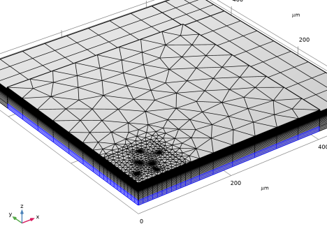
Click to expand the Coloring and Style section. Find the Line style subsection. From the Line list, choose None.
10
Find the Line markers subsection. From the Marker list, choose Point.
11
In the Sensitivity toolbar, click  Plot.
Due to the significant dependence of the frequency shift on the particle attachment location as discussed earlier, it is not possible to arrive at an exact sensitivity number (frequency shift per added particle mass), as evidenced by the scatter of the data points in the graph. A rough number of about 10 MHz/ng can be estimated from the graph.
Add a study to compare the frequency response with versus without particles attached. The frequency list is tailored to only show the main resonance.
Add Study
1
In the Home toolbar, click  Add Study to open the Add Study window.
2
Go to the Add Study window.
3
Find the Studies subsection. In the Select Study tree, select General Studies>Frequency Domain.
4
Click Add Study in the window toolbar.
5
In the Home toolbar, click  Add Study to close the Add Study window.
Study 2
Step 1: Frequency Domain
1
In the Settings window for Frequency Domain, locate the Study Settings section.
2
From the Frequency unit list, choose MHz.
3
Click  Range.
4
In the Range dialog box, type 870.3 in the Start text field.
5
In the Step text field, type 0.05.
6
In the Stop text field, type 870.9.
7
Click Replace.
8
In the Model Builder window, click Study 2.
9
In the Settings window for Study, type Study 2 - Frequency response in the Label text field.
Parametric Sweep
1
In the Study toolbar, click  Parametric Sweep.
2
In the Settings window for Parametric Sweep, locate the Study Settings section.
3
4
5
6
7
8
9
10
11
12
13
14
15
In the Study toolbar, click  Compute.
Take a look at the electric potential solution at the main resonance.
Results
Electric Potential (es) 1
1
In the Model Builder window, under Results click Electric Potential (es) 1.
2
In the Settings window for 3D Plot Group, locate the Data section.
3
From the Parameter value (p1,p2,p3,p4,p5,p6) list, choose 1: p1=0, p2=0, p3=0, p4=0, p5=0, p6=0.
4
From the Parameter value (freq (MHz)) list, choose 870.75.
Multislice 1
1
In the Model Builder window, expand the Electric Potential (es) 1 node.
2
Right-click Multislice 1 and choose Disable.
Streamline Multislice 1
In the Model Builder window, right-click Streamline Multislice 1 and choose Disable.
Volume 1
1
In the Model Builder window, right-click Electric Potential (es) 1 and choose Volume.
2
In the Settings window for Volume, locate the Expression section.
3
In the Expression text field, type V.
4
In the Electric Potential (es) 1 toolbar, click  Plot.
Add plots of the impedance to look at the frequency response curves with and without particles. The resonance peak shifts to lower frequency with added particles as expected.
Frequency Response
1
In the Home toolbar, click  Add Plot Group and choose 1D Plot Group.
2
In the Settings window for 1D Plot Group, type Frequency Response in the Label text field.
3
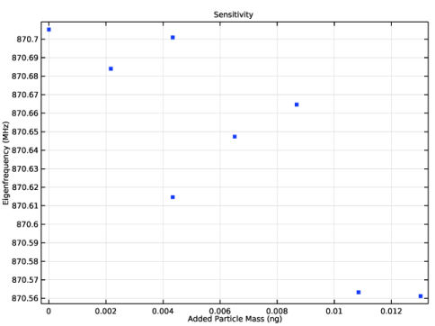
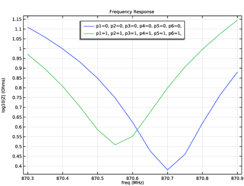
Locate the Data section. From the Dataset list, choose Study 2 - Frequency response/Parametric Solutions 1 (sol3).
4
Locate the Title section. From the Title type list, choose Label.
5
Locate the Legend section. From the Position list, choose Upper middle.
Global 1
1
Right-click Frequency Response and choose Global.
2
In the Settings window for Global, locate the y-Axis Data section.
3
4
In the Frequency Response toolbar, click  Plot.