Equation 3-37 in the section
Electrons in a Perturbed Periodic Potential describes the transport of both electrons and holes in a semiconductor with a potential that varies in space. In many circumstances the potential varies slowly in space and wave packets move according to the classical Hamiltonian, so correspondingly their dynamics is determined by the semiclassical model, from which both drift-diffusion equations follow. However, since
Equation 3-37 is essentially a Schrödinger equation for electrons and holes, it allows for quantum mechanical phenomena such as tunneling, which are outside of the scope of the semiclassical model.
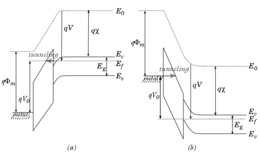
Tunneling occurs when an electron or hole wave packet is incident on a narrow potential barrier with a barrier height greater than the energy associated with the group velocity of the wave packet. A classical particle would be reflected at the boundary, but in the solutions of the Schrödinger equation the envelope function Ψm(
r) associated with the wave packet decays exponentially inside the barrier. For thin barriers,
Ψm(
r) is significant on the opposite side of the barrier, and correspondingly there is a transmission probability associated with transport through the potential barrier. Since the tunneling probability must be computed for wave packets with a range of energies or
k-vectors, it is usually only possible to solve the tunneling problem in 1D. Consequently, the approaches adopted are necessarily phenomenological in nature. The nature of the approximations required to arrive at the theory of tunneling is discussed in detail in section 4 of
Ref. 42. Since much of the underlying theory is approximate in nature, it is sensible to favor numerically lighter solutions over more detailed approaches.
Fowler and Nordheim originally treated tunneling through triangular barriers (Ref. 43) in the context of the Sommerfeld model. Their analysis was applied to tunneling in oxides within a semiconductor device context by Lenzlinger and Snow (
Ref. 44). It is worth noting that Fowler and Nordheim did not make a WKB approximation in their original analysis, but instead approximated the final form of the analytic solution (a WKB approximation was used in
Ref. 44 but for this reason is not strictly necessary). The original result due to Fowler and Nordheim showed that the tunnel current through a triangular barrier for electrons (

) and/or holes (

) takes the form:
where Eins is the electric field in the insulator and

,

,

, and

are constants related to the material properties of the insulator and semiconductor. For the commonly encountered case of the silicon/silicon oxide system, only electron tunneling needs to be considered because the barrier for hole tunneling is significantly higher than that for electrons.
Ref. 44 provides a detailed derivation of
Equation 3-148, for the case of a semiconductor-oxide system at finite temperature. The effect of a finite temperature was shown to be equivalent to a change in the values of the constants

and

. Similarly image force lowering effects at the barrier also caused an effective change in these constants. Since using the derivative material properties does not lead to a fully consistent description of the tunneling current as a function of both electric field and temperature, it is customary to simply treat

and

as inputs to a model of the tunneling process at a particular temperature. These values can be extracted from a plot of
log(
/
Eins2) versus 1/
Eins.