
|
|
|


|
1
|
|
2
|
|
3
|
Click Add.
|
|
4
|
Click
|
|
5
|
|
6
|
Click
|
|
1
|
|
2
|
|
1
|
|
2
|
|
3
|
Click
|
|
4
|
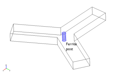
Browse to the model’s Application Libraries folder and double-click the file circulator.mphbin.
|
|
5
|
Click
|
|
6
|
|
1
|
|
2
|
|
3
|
In the tree, select Built-in>Air.
|
|
4
|
|
5
|
|
1
|
|
2
|
|
4
|
|
1
|
|
2
|
|
4
|
|
5
|
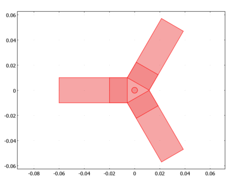
In the Model Builder window, expand the Component 1 (comp1)>Materials>Ferrite (mat3) node, then click Basic (def).
|
|
6
|
|
7
|
|
8
|
|
9
|
Click
|
|
10
|
|
11
|
Click OK.
|
|
12
|
|
13
|
In the Local properties table, enter the following settings:
|
|
1
|
In the Model Builder window, under Component 1 (comp1) click Electromagnetic Waves, Frequency Domain (emw).
|
|
2
|
|
3
|
|
1
|
|
3
|
|
4
|
|
1
|
|
3
|
|
4
|
|
1
|
|
3
|
|
4
|
|
1
|
|
2
|
|
3
|
|
4
|
|
5
|
|
1
|
|
2
|
|
3
|
Click
|
|
1
|
|
2
|
|
3
|
|
4
|
|
1
|
|
2
|
|
3
|
|
4
|
|
5
|
|
1
|
|
2
|
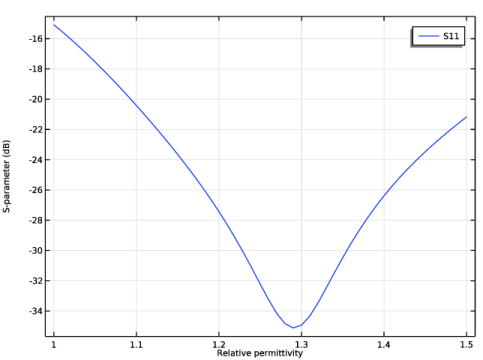
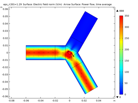
In the Settings window for Arrow Surface, click Replace Expression in the upper-right corner of the Expression section. From the menu, choose Component 1 (comp1)>Electromagnetic Waves, Frequency Domain>Energy and power>emw.Poavx,emw.Poavy - Power flow, time average.
|
|
3
|
Locate the Arrow Positioning section. Find the Y grid points subsection. In the Points text field, type 25.
|
|
4
|
|
5
|
|
1
|
|
2
|
In the Settings window for Global, click Replace Expression in the upper-right corner of the y-Axis Data section. From the menu, choose Component 1 (comp1)>Electromagnetic Waves, Frequency Domain>Ports>S-parameter, dB>emw.S11dB - S11.
|
|
3
|
|
1
|
|
2
|
|
3
|
|
4
|