|
|
|
|
1
|
|
2
|
|
3
|
Click Add.
|
|
4
|
Click
|
|
5
|
|
6
|
Click
|
|
1
|
|
2
|
|
3
|
|
1
|
|
2
|
|
1
|
|
2
|
|
1
|
|
2
|
|
3
|
|
1
|
|
2
|
|
3
|
|
4
|
|
5
|
|
1
|
|
2
|
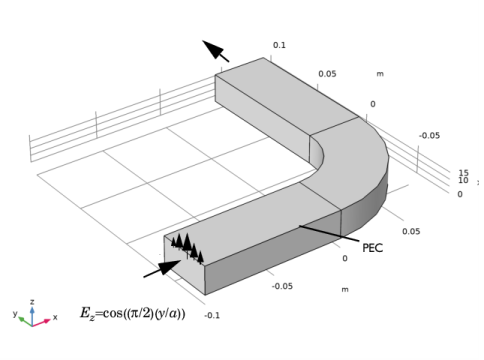
Select the object c2 only.
|
|
3
|
|
4
|
|
5
|
Select the object c1 only.
|
|
1
|
|
2
|
|
3
|
|
4
|
|
5
|
|
1
|
|
2
|
|
3
|
|
4
|
|
5
|
|
6
|
|
7
|
|
1
|
In the Model Builder window, under Component 1 (comp1)>Geometry 1 right-click Work Plane 1 (wp1) and choose Extrude.
|
|
2
|
|
4
|
|
5
|
|
1
|
In the Model Builder window, under Component 1 (comp1)>Electromagnetic Waves, Frequency Domain (emw) click Wave Equation, Electric 1.
|
|
2
|
|
3
|
|
1
|
|
3
|
|
4
|
|
1
|
|
3
|
|
4
|
|
1
|
In the Model Builder window, under Component 1 (comp1) right-click Materials and choose Blank Material.
|
|
2
|
|
4
|
|
1
|
|
2
|
|
4
|
|
1
|
|
1
|
|
2
|
|
3
|
|
4
|
|
1
|
|
2
|
|
3
|
|
4
|
|
1
|
|
2
|
|
1
|
|
2
|
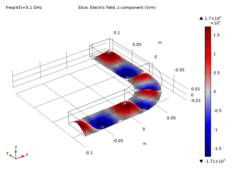
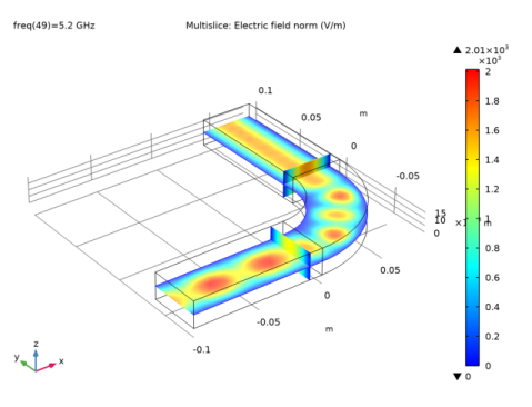
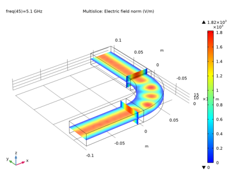
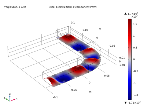
In the Settings window for Slice, click Replace Expression in the upper-right corner of the Expression section. From the menu, choose Component 1 (comp1)>Electromagnetic Waves, Frequency Domain>Electric>Electric field - V/m>emw.Ez - Electric field, z component.
|
|
3
|
|
4
|
|
5
|
|
6
|
|
7
|
Click to expand the Range section. Locate the Coloring and Style section. From the Scale list, choose Linear symmetric.
|
|
1
|
|
2
|
In the Settings window for Deformation, click Replace Expression in the upper-right corner of the Expression section. From the menu, choose Component 1 (comp1)>Electromagnetic Waves, Frequency Domain>Electric>emw.Ex,emw.Ey,emw.Ez - Electric field.
|
|
3
|
|
1
|
In the Model Builder window, under Component 1 (comp1) click Electromagnetic Waves, Frequency Domain (emw).
|
|
2
|
In the Settings window for Electromagnetic Waves, Frequency Domain, locate the Port Sweep Settings section.
|
|
3
|
|
4
|
Click Configure Sweep Settings. By clicking the Configure Sweep Settings button, all necessary port sweep settings such as sweep parameter and parametric study step will be automatically added. It is necessary to run the parametric sweep with port names to get a full S-parameter matrix.
|
|
5
|
|
6
|
Click the Browse button and select a file to which you want to export the results in the Touchstone format. If the file does not exist, it will be created.
|
|
1
|
|
2
|
|
3
|
|
4
|
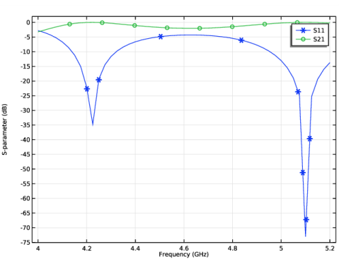
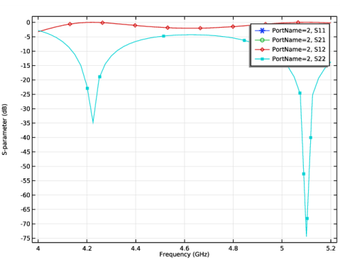
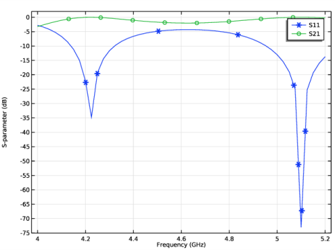
Click Add Expression in the upper-right corner of the y-Axis Data section. From the menu, choose Component 1 (comp1)>Electromagnetic Waves, Frequency Domain>Ports>S-parameter, dB>emw.S12dB - S12.
|
|
5
|
Click Add Expression in the upper-right corner of the y-Axis Data section. From the menu, choose Component 1 (comp1)>Electromagnetic Waves, Frequency Domain>Ports>S-parameter, dB>emw.S22dB - S22.
|
|
6
|
|
7
|
|
1
|
|
2
|
|
3
|
|
4
|
|
1
|
|
2
|
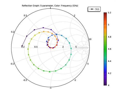
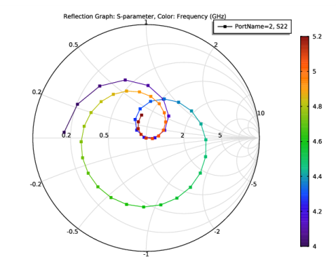
In the Settings window for Reflection Graph, click Replace Expression in the upper-right corner of the Expression section. From the menu, choose Component 1 (comp1)>Electromagnetic Waves, Frequency Domain>Ports>S-parameter>emw.S22 - S22.
|
|
3
|
|
1
|
|
2
|
|
3
|