|
|
|
|
1
|
|
2
|
Click
|
|
1
|
|
2
|
|
3
|
Click Browse.
|
|
4
|
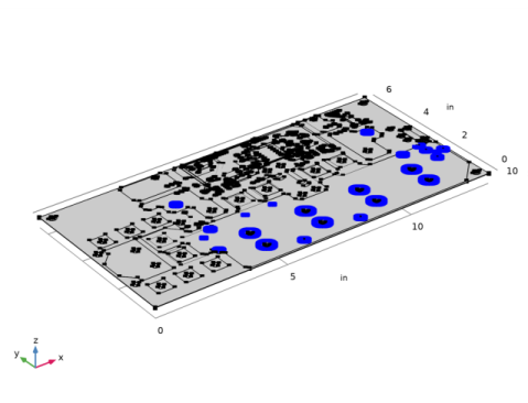
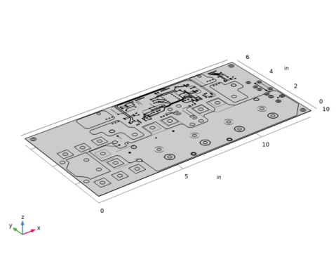
Browse to the model’s Application Libraries folder and double-click the file printed_circuit_board_si_geom.zip.
|
|
5
|
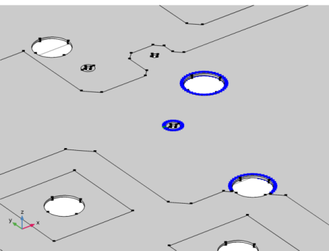
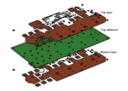
Find the Layers to import subsection. In the table, select to import only the following layers:
|
|
6
|
|
7
|
|
8
|
Click Import.
|
|
1
|
|
2
|
|
1
|
|
2
|
|
3
|
|
1
|
|
2
|
|
3
|
|
4
|
Click
|
|
5
|
|
6
|
|
1
|
|
2
|
|
3
|
|
4
|
|
5
|
In the Add dialog box, in the Selections to add list, choose TOP (Import 1), BOTTOM (Import 1), and TOP.DIEL (Import 1).
|
|
6
|
Click OK.
|
|
7
|
|
8
|
|
9
|
|
1
|
|
2
|
|
3
|
|
4
|
|
5
|
In the Add dialog box, in the Selections to add list, choose TOP (Import 1), BOTTOM (Import 1), and DRILL.TOP.DIEL (Import 1).
|
|
6
|
Click OK.
|
|
7
|
|
1
|
|
2
|
|
3
|
|
4
|
|
1
|
|
2
|
|
3
|
|
4
|
|
5
|
|
6
|
|
1
|
|
2
|
|
3
|
|
4
|
|
5
|
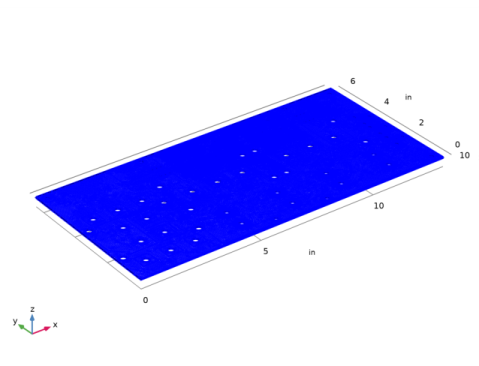
In the tree, select Built-in>Copper.
|
|
6
|
|
7
|
|
1
|
|
2
|
|
1
|
|
2
|
|
3
|
|
4
|
|
5
|
|
1
|
|
1
|
|
2
|
|
3
|
In the list, select 317.
|
|
4
|
|
5
|
|
6
|
|
7
|
|
1
|
|
2
|
|
3
|
|
4
|
|
5
|
|
6
|
|
7
|
|
8
|
|
9
|
|
10
|
|
11
|
|
1
|
|
2
|
|
3
|
|
4
|
In the list, select 237.
|
|
5
|
|
6
|
|
1
|
|
2
|
|
3
|
|
4
|
|
1
|
|
2
|
|
3
|
|
1
|
|
2
|
|
3
|
Click the Custom button.
|
|
4
|
|
5
|
|
1
|
|
2
|
|
3
|
|
4
|
|
5
|
|
6
|
|
7
|
In the associated text field, type 0.1[in].
|
|
8
|
|
9
|
In the associated text field, type 0.01[in].
|
|
10
|
|
11
|