PDF

Modeling a Capacitive Position Sensor Using FEM
Introduction
In this electrostatics tutorial model the capacitance matrix of a five-terminals sensor is computed and related to the position of a metallic test object. The model explains how to extract lumped matrices using the Stationary Source Sweep Study. Useful extra features of the Stationary Source Sweep Study, such as sweeping on a subset of the terminals are showcased. It is also discussed how the study’s performance is affected when using direct and iterative solvers.
Model Definition
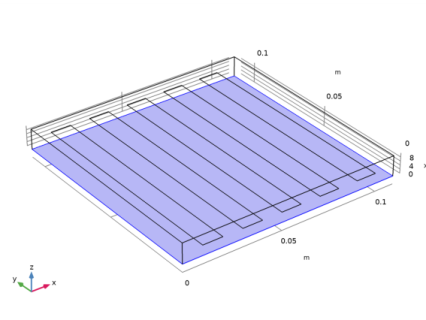
The model solves an electrostatic problem typical for the design of capacitive position sensors. A generic design consists of a ground plane (Figure 1), and a series of electrodes (Figure 2).
Figure 1: The ground plane of the sensor is highlighted.
Figure 2: The five sensing electrodes are highlighted.
Figure 3: Test object when it is far from the sensor.
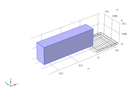
Any metallic object or object with dielectric contrast in the neighborhood of the sensor will change the capacitive coupling between the electrodes, including the ground electrode (Figure 3 and Figure 4).
Figure 4: Test object when it is approaching the sensor.
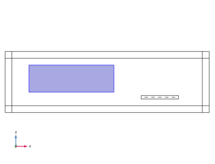
This version of the model uses the finite element method. It requires adding a domain to model the air in between the sensor and the object and some of the surrounding air to capture fringing fields (see Figure 5). The dipole field surrounding the sensor falls off quickly with distance so it is possible to limit the computational domain to a high degree. The related model Modeling a Capacitive Position Sensor Using BEM considers the case of the whole object in infinite space.
Figure 5: Truncation of the computational domain and test object.
In the Stationary Source Sweep study, COMSOL Multiphysics identifies all Terminal features in the model and excites them one at a time using a fixed charge excitation. The Terminals not excited are left at a floating potential (zero net charge).
The Stationary Source Sweep study generates default output nodes for three variants of the capacitance matrix: inverse Maxwell capacitance matrix (also known as the elastance matrix), Maxwell capacitance matrix, and the mutual capacitance matrix (also known as the SPICE capacitance matrix). For details, see the sections on Lumped Parameter Conversion and Stationary Source Sweep in the AC/DC Module User’s Guide.
Depending on the electronics triggering the presence of the object, any of the three capacitance matrices may be the most relevant.
The surface of the metallic test object is modeled using domain Terminal condition with zero charge (floating electrode). It is shown how to exclude this extra Terminal from the sweep made at the study level.
The Stationary Source Sweep is optimized for solution speed. It works best with a direct solver as the LU decomposition has to be performed only once, followed by back substitution for the multiple source excitations (multiple right-hand sides). For 3D models, the Stationary Source Sweep generates both an iterative and a direct solver. The former will be selected if the model is having a large number of elements, that is, above a built-in threshold. For hardware with sufficiently large RAM, it is recommended to manually switch to the direct solver.
Results and Discussion
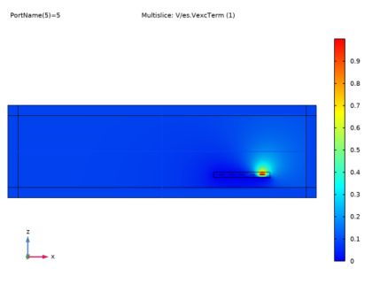
Figure 6 shows the default plot of the scaled Electric potential in absence of the test object when one of the lateral terminals is fed. The potential is zero at ground and the plot quantity is scaled to be unity at the excited terminal. In the step by step instructions, other similar plot are produced for the other terminals. While, one terminal is fed, the floating potential values of the non excited terminals are nonzero. These values represent measures of the off diagonal cross-capacitance couplings between different terminals.
Figure 6: Electric potential in absence of the test object when one of the lateral terminals is fed.
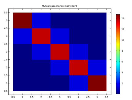
The default matrix generation works by aggregating all data on all terminals and the results are presented in tables. Data in a table, can also be plotted, see Figure 7.
Figure 7: Mutual capacitance matrix displayed in a 2D plot.
The presence of the metallic test object influences the electric potential as can be clearly seen by comparing Figure 8 and Figure 9. Figure 8 resembles Figure 6 where the test object is absent. Figure 9 shows how the electric potential drop, that is the electric field, is confined to a much more narrow region. This changes the accumulated surface charge on the conductors.
Figure 8: Electric potential in the presence of the test object in a position far from the sensor, when the nearest terminals is fed.
Figure 9: Electric potential in the presence of the test object in a position near the sensor, when the nearest terminals is fed.
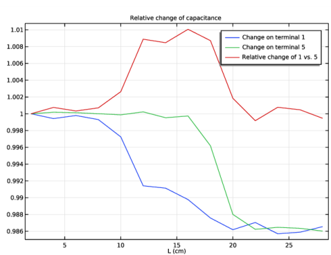
A sensor is equipped with feeding circuitry that is designed to detect changes to the electrode to ground capacitance and/or interelectrode capacitances, thereby detecting the presence and position of an object. Many different combinations are possible. In Figure 10, three evaluations of the change in capacitance are shown. The blue and green curves represent the change in inverse self capacitance of the most near and the most far electrode as a function of the position of the test object. Both electrodes change their absolute capacitances by about 2% when the object is approaching their positions. The most near sensor start sensing a change at a position of L = 0.1 m while the other start sensing the change when L = 0.15 m. The absolute capacitance of an electrode can slowly drift, for example because of water absorption in the dielectric. For this reason, it is more interesting to detect the presence of the object by means of relative changes in interelectrode capacitance values. The relative change in elastance of the first versus the last electrode is reported as the red curve in Figure 10. It is clear that the test object produces a change in response of the nearest electrode with respect to the farmost one. This can trigger properly designed feeding circuitry detecting the presence of the object.
Figure 10: Change in inverse capacitance (elastance) as function of position of the incoming metal object. Blue and green line are respectively the absolute change of the most near and the most far electrode. Red line is the relative change of the most near versus the most far electrode.
Application Library path: ACDC_Module/Tutorials/capacitive_position_sensor
Modeling Instructions
From the File menu, choose New.
New
In the New window, click  Model Wizard.
Model Wizard
1
In the Model Wizard window, click  3D.
2
In the Select Physics tree, select AC/DC>Electric Fields and Currents>Electrostatics (es).
3
Click Add.
4
In the Added physics interfaces tree, select Electrostatics (es).
5
Click  Study.
The following steps add the Stationary Source Sweep study step that automatically extracts the capacitance matrices for an N-port system, which is the final aim of this model.
6
In the Select Study tree, select Preset Studies for Selected Physics Interfaces>Stationary Source Sweep.
7
Geometry 1
Add the nylon block with the five embedded rectangular electrodes.
Block 1 (blk1)
1
In the Geometry toolbar, click  Block.
2
In the Settings window for Block, locate the Size and Shape section.
3
In the Width text field, type 11[cm].
4
In the Depth text field, type 11[cm].
5
In the Height text field, type 1[cm].
Work Plane 1 (wp1)
1
In the Geometry toolbar, click  Work Plane.
2
In the Settings window for Work Plane, locate the Plane Definition section.
3
In the z-coordinate text field, type 5[mm].
4
Click  Show Work Plane.
Work Plane 1 (wp1)>Rectangle 1 (r1)
1
In the Work Plane toolbar, click  Rectangle.
2
In the Settings window for Rectangle, locate the Size and Shape section.
3
In the Width text field, type 1[cm].
4
In the Height text field, type 11[cm].
5
Locate the Position section. In the xw text field, type 1[cm].
Work Plane 1 (wp1)>Array 1 (arr1)
1
In the Work Plane toolbar, click  Transforms and choose Array.
2
3
In the Settings window for Array, locate the Size section.
4
In the xw size text field, type 5.
5
Locate the Displacement section. In the xw text field, type 2[cm].
Work Plane 1 (wp1)
1
In the Model Builder window, click Work Plane 1 (wp1).
2
In the Settings window for Work Plane, click  Build Selected.
Add an enclosing box for modeling the external air domain and add the corresponding materials.
Block 2 (blk2)
1
In the Geometry toolbar, click  Block.
2
In the Settings window for Block, locate the Size and Shape section.
3
In the Width text field, type 60[cm].
4
In the Depth text field, type 18[cm].
5
In the Height text field, type 18[cm].
6
Locate the Position section. In the x text field, type -40[cm].
7
In the y text field, type -4[cm].
8
In the z text field, type -4[cm].
After having built the air box, add a layer on its sides where Infinite Elements are specified.
9
Click to expand the Layers section. In the table, enter the following settings:
10
Find the Layer position subsection. Select the Left check box.
11
Select the Right check box.
12
Select the Front check box.
13
Select the Back check box.
14
Select the Top check box.
15
Click  Build Selected.
16
Click the  Zoom Extents button in the Graphics toolbar.
Definitions
Infinite Element Domain 1 (ie1)
1
In the Definitions toolbar, click  Infinite Element Domain.
2
Add Material
1
In the Home toolbar, click  Add Material to open the Add Material window.
2
Go to the Add Material window.
3
4
Click  Add to Component 1 (comp1).
5
In the tree, select Built-in>Nylon.
6
Click  Add to Component 1 (comp1).
7
In the Home toolbar, click  Add Material to close the Add Material window.
Materials
Nylon (mat2)
Select Domain 19 only.
Electrostatics (es)
Ground 1
Apply ground and the five boundary terminal conditions.
1
In the Model Builder window, under Component 1 (comp1) right-click Electrostatics (es) and choose Ground.
2
Repeat the following two operations five times for adding the five terminals. Select boundary 12, 13, 14, and 15 for terminal 2, 3, 4, and 5, respectively.
Terminal 1
1
In the Physics toolbar, click  Boundaries and choose Terminal.
2
As stated above, repeat the two operations above four times more, to create the remaining four terminals.
The Physics Controlled Mesh creates a proper swept mesh for the Infinite Elements. However, refine the mesh element size and run the model.
Mesh 1
1
In the Model Builder window, under Component 1 (comp1) click Mesh 1.
2
In the Settings window for Mesh, locate the Physics-Controlled Mesh section.
3
From the Element size list, choose Finer.
Study 1
In the Home toolbar, click  Compute.
Look at the potential when terminal 5 is fed.
Results
Electric Potential (es)
Repeat the following operations to look at the potential when each of the other four terminals are fed. The results should look as in the following plot.
4
In the Settings window for 3D Plot Group, click  Plot Previous.
You can easily generate the inverse capacitance matrix, the Maxwell capacitance matrix, and mutual capacitance matrix by just a few clicks.
5
In the Results toolbar, click  Evaluate and choose Clear and Evaluate All.
Maxwell capacitance (es, dset1)
As the capacitances are really small numbers in the base SI unit, F, they can be postprocessed in pF by the following steps.
1
In the Model Builder window, expand the Results>Derived Values node, then click Maxwell capacitance (es, dset1).
2
In the Settings window for Global Matrix Evaluation, locate the Expression section.
3
From the Unit list, choose 1/pF.
Mutual capacitance (es, dset1)
1
In the Model Builder window, click Mutual capacitance (es, dset1).
2
In the Settings window for Global Matrix Evaluation, locate the Expression section.
3
From the Unit list, choose 1/pF.
4
In the Results toolbar, click  Evaluate and choose Clear and Evaluate All.
Finally, it is possible to postprocess these matrix entries also as a table plot. To do this, follow the next instructions.
Table
1
Go to the Table window.
2
Click Table Surface in the window toolbar.
Results
Table Surface 1
1
In the Model Builder window, under Results>2D Plot Group 2 click Table Surface 1.
2
In the Settings window for Table Surface, locate the Data section.
3
From the Data format list, choose Cells.
4
Locate the Coloring and Style section. From the Function list, choose Discrete.
5
In the 2D Plot Group 2 toolbar, click  Plot.
6
Click the  Zoom Extents button in the Graphics toolbar.
2D Plot Group 2
1
In the Model Builder window, click 2D Plot Group 2.
2
In the Settings window for 2D Plot Group, click to expand the Title section.
3
From the Title type list, choose Manual.
4
In the Title text area, type Mutual capacitance matrix [pF].
5
In the 2D Plot Group 2 toolbar, click  Plot.
6
Click the  Zoom Extents button in the Graphics toolbar. The result should look like Figure 7 in the introduction.
Configuration of a direct solver
If the model is not particularly big for the employed computer, the next instructions show how to switch from iterative solver to direct solver. If the model was detected to be sufficiently small, the direct solver would have been the default.
Study 1
Solver Configurations
In the Model Builder window, expand the Study 1>Solver Configurations node.
Solution 1 (sol1)
1
In the Model Builder window, expand the Study 1>Solver Configurations>Solution 1 (sol1)>Stationary Solver 1 node.
2
Right-click Direct and choose Enable.
Now, solve and inspect the results and verify that the results have not changed.
3
In the Home toolbar, click  Compute.
Results
1
In the Results toolbar, click  Evaluate and choose Clear and Evaluate All.
Conversely, if there is the need to decrease amount of required RAM, it is possible to manually enable the iterative solver.
Sensing the position of a metal billet
To model a copper metal billet entering the system and reaching different positions, a block is added with a parameterized position. A terminal, providing an equipotential boundary condition, is added to this block. Notice that the instruction includes also the addition of the material. This is not stricly necessary as the terminal condition would be enough for describing the conductor.
Global Definitions
Parameters 1
1
In the Model Builder window, under Global Definitions click Parameters 1.
2
In the Settings window for Parameters, locate the Parameters section.
3
Geometry 1
Block 3 (blk3)
1
In the Geometry toolbar, click  Block.
2
In the Settings window for Block, locate the Size and Shape section.
3
In the Width text field, type 25[cm].
4
In the Depth text field, type 5[cm].
5
In the Height text field, type 8[cm].
6
Locate the Position section. In the x text field, type -35[cm]+L.
7
In the y text field, type 3[cm].
8
In the z text field, type 2[cm].
9
Click  Build Selected.
Add Material
1
In the Home toolbar, click  Add Material to open the Add Material window.
2
Go to the Add Material window.
3
In the tree, select Built-in>Copper.
4
Click  Add to Component 1 (comp1).
5
In the Home toolbar, click  Add Material to close the Add Material window.
Materials
Copper (mat3)
Select Domain 19 only.
Electrostatics (es)
The fastest way to model an electrically floating solid metal object is by adding a sixth terminal, where zero charge is specified. This is simply done adding a domain Terminal.
Terminal 6
1
In the Physics toolbar, click  Domains and choose Terminal.
2
When clicking Compute now, a sweep over the six terminals is performed.
Study 1
In the Home toolbar, click  Compute.
Results
In the Results toolbar, click  Evaluate and choose Clear and Evaluate All.
To exclude the block from the sweep, it is enough to modify the settings in the Solve only for specified sources section.
Study 1
Step 1: Stationary Source Sweep
1
In the Model Builder window, under Study 1 click Step 1: Stationary Source Sweep.
2
In the Settings window for Stationary Source Sweep, locate the Source Selection section.
3
Select the Solve only for specified sources check box.
4
In the Source names text field, type range(1,1,5).
5
In the Home toolbar, click  Compute.
Results
Electric Potential (es)
Regenerating the capacitance matrices, it is possible to appreciate that they are really similar to the initial case. The discrepancies are due mainly to the effect of the new conducting domain, which is currently far from the system and thereby not influencing its capacitive behavior.
1
In the Results toolbar, click  Evaluate and choose Clear and Evaluate All.
Parametric sweep for different billet positions
Add a Parametric Sweep controlling the metal billet displacement parameter L.
Study 1
Parametric Sweep
1
In the Study toolbar, click  Parametric Sweep.
2
In the Settings window for Parametric Sweep, locate the Study Settings section.
3
4
5
In the Study toolbar, click  Compute.
Results
Electric Potential (es) 1
The next instructions explain how to specify the position of the metal billet in the plot of the normalized electric potential.
1
In the Settings window for 3D Plot Group, locate the Data section.
2
From the Parameter value (PortName) list, choose 1.
Finally, it is shown how to generate a 1D plot of the capacitance response for different positions.
1D Plot Group 4
1
In the Home toolbar, click  Add Plot Group and choose 1D Plot Group.
2
In the Settings window for 1D Plot Group, locate the Data section.
3
From the Dataset list, choose Study 1/Parametric Solutions 1 (sol2).
4
Click to expand the Title section. From the Title type list, choose Manual.
5
In the Title text area, type Relative change of capacitance.
Global 1
1
Right-click 1D Plot Group 4 and choose Global.
2
In the Settings window for Global, locate the Data section.
3
From the Dataset list, choose Study 1/Parametric Solutions 1 (sol2).
4
From the Parameter selection (PortName) list, choose First.
5
Locate the x-Axis Data section. From the Axis source data list, choose L.
6
Locate the y-Axis Data section. In the table, enter the following settings:
7
Click to expand the Legends section. From the Legends list, choose Manual.
8
9
In the 1D Plot Group 4 toolbar, click  Plot. The resulting plot will look like Figure 10 in the introduction.