You are viewing the documentation for an older COMSOL version. The latest version is
available here.
(3-8)

where n1,
n2,
and
n3 are integers (taking all values between –
∞ and
∞) and
a1,
a2,
and
a3 are the lattice vectors. For a primitive lattice, the unit cell is the parallelepiped constructed from the vectors
a1,
a2,
and
a3.
where a is the lattice parameter. This periodic function can be represented by a Fourier series of the form:
(3-9)

Of particular importance to understand semiconductor transport is the concept of the reciprocal lattice. This is the lattice produced by taking the Fourier transform of the real space lattice. For the Dirac comb this is given by:
where the final step follows from Equation 3-9. The reciprocal lattice is another Dirac comb with spacing proportional to the reciprocal of the real space lattice.
In 3D the lattice can be represented as δ (
r–
R) where the summation over all combinations of lattice vectors is implied by the use of the set of vectors
R. The Fourier transform of the lattice is:
where Ω is the volume of the real space unit cell (
Ω = a1 ⋅ (
a2 × a3)) and
K*is the set of reciprocal lattice vectors given by:
where n1,
n2,
and
n3 are integers (taking all values between –
∞ and
∞) and
b1,
b2,
and
b3 are the reciprocal lattice vectors given by:
(3-10)

Understanding the reciprocal lattice in terms of Fourier transforms as described above is useful. The Heisenberg uncertainty principle can be seen to be related to the properties of the Fourier transform (in the time domain: ΔfΔt≈1). Also the effect of a lattice basis can be straightforwardly introduced by taking the convolution of the basis with the lattice in real space. The convolution theorem then tells us that the result in reciprocal space (or k-space) is the product of the reciprocal lattice and the Fourier transform of the basis. The main effect of the basis is to modulate the amplitude (and phase) of the reciprocal lattice points. When zeros in the Fourier transform of the basis coincide with reciprocal lattice points, the basis leads to the elimination of these points in the reciprocal lattice. In X-ray imaging experiments, which sample the reciprocal lattice by crystal diffraction, this is referred to as
extinction.
(3-11)

where the summation occurs over all the reciprocal lattice vectors K*. The reciprocal lattice is therefore a representation of the Fourier components required in 3D to represent a function with the periodicity of the lattice.
(3-12)

which leads to the requirement that θ depends linearly on the three integers,
n1,
n2, and
n3, which specify
R (see
Equation 3-8):
θ can therefore be written in the form:
for constants c1,
c2, and
c3. Writing
k = c1b1 + c2b1 + c3b1 leads to the requirement
θ = k⋅R and
Equation 3-12 then becomes:
(3-13)

If ψ (
r) is written in the form:
(3-14)

substituting into Equation 3-13 shows that
uk(
r+R)
= uk(
r).
Equation 3-14, along with the periodicity requirement on
uk(
r), is known as
Bloch’s theorem. It is extremely useful as it allows the wave function corresponding to a particular
k vector to be expanded in a Fourier series of the same form as that of the potential (
Equation 3-11):
where G is used for the potential reciprocal lattice vector to distinguish it from
K. Simplifying this equation gives:
(3-15)

Equation 3-15 is valid for any periodic potential, small or large.
To obtain the small potential limit of Equation 3-15, consider the case of a single sinusoidal potential component with a small amplitude:
and Equation 3-15 takes the form:
(3-16)

In the limit V1 = 0,
p = 0, and
Equation 3-16 recovers the form of the Sommerfeld
E-k relationship,
Equation 3-4. However, for
V1 = 0, additional solutions now also exist for nonzero values of
p, which take the form of a set of parabolas with origins shifted by
p times the reciprocal lattice vector
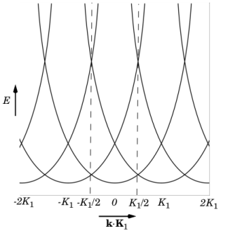
K1. As a result of the periodicity of the lattice,
E has become multivalued for a given
k as shown in
Figure 3-1. The
E-k relationship is periodic, with a single repeating unit contained within the dashed lines (shown at
±K1/2). Since the parts of the plot outside the dashed lines consist of repeated information,
Ek plots are conventionally drawn showing only the region between the dashed lines. This region is called the Brillouin zone and in 3D it consists of all the points in k-space closer to one particular reciprocal lattice point
K than to any other point.
Writing Equation 3-16 explicitly for the case
V1 = 0 gives:
(3-17)

Figure 3-1 shows that on the planes half between the lattice vectors (defined by the equations
k·
K1 = qK1/2, for integers
q, and indicated by the dashed line), the energy associated with two different values of
p, for example
p1 and
p2, can be equal. Note that
p1 and
p2 are associated with two (different) periodic components of the wave function or with two different
Ek curves in the figure. Away from these planes, the energy associated with each periodic component of the wave function differs from all the other components.
Next consider the energy on the plane k·
K1 = qK1/2, at the point corresponding to
p1 = 0 and
p2 = 1 as
Equation 3-17 changes into
Equation 3-16 by a slow increase of
V1 from zero. Close to the plane it is expected that initially, as
V1 is increased, a solution exists in which
C0 and
C1 are significant but all other coefficients are extremely small; that is, a solution in which only the
p1 = 0 and
p2 = 1 components of the wave function play a significant role. Making the assumption that the other coefficients are zero reduces the set of
Equation 3-16 to just two equations:
where the vector k has been decomposed into components parallel (
k||) and perpendicular (
k⊥) to
K1. Taking the product of these two equations leads to a quadratic equation that can be solved to obtain the value of
E. It is most convenient to use the following nondimensional variables when solving the equation:
(3-18)

In the case U = 0
, k⊥= 0, this equation reproduces the two parabolas centered on 0 and
K1 (
Figure 3-1). A nonzero value of
k⊥ simply shifts the parabolas to greater energies. At the edge of the
Brillouin zone (indicated by the dashed line), where the two parabolas cross,
δ is zero, and as
k|| decreases,
δ increases, reaching a maximum of 1 at the origin. When a small but finite value of
U is introduced (for example
U < 0.1) there is little effect on the curve away from the Brillouin zone edge, but as
δ becomes comparable to, or less than,
U its effect becomes significant. At the edge of the Brillouin zone the two
Ek curves (corresponding to two different Fourier components of the wave function) no longer cross but are separated by a small gap such that
ε=1
±U. This corresponds to a gap between the lowest two
Ek curves of magnitude 2
V1.
The form of Equation 3-16 makes it clear what the effect of other harmonics in the periodic potential would be. For a potential of the form:
The effect of Vh is to couple the equations involving
Cp and
Cp±h, and it therefore perturbs apart the parabolas centered on
pK1 and on (
p ± h)
K1. Provided
Vh is small, its effect is only significant near the edge of the Brillouin zone. Thus, for a more general periodic potential with higher harmonics, the
Ekrelationship takes the form shown in
Figure 3-2.
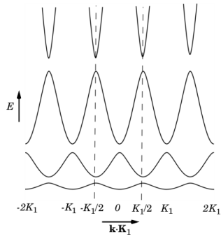
The Ek diagram has now changed so that certain energies are forbidden. The allowed states exist within bands of permitted energies, with
band gaps separating them.
Figure 3-2 can be redrawn in various ways. In the figure the repeated zone scheme is shown. This scheme highlights the periodicity of the lattice and makes clear the concept of energy bands and band gaps. An alternative is to show only the
nth band in the
nth Brillouin zone (known as the extended band scheme). This approach produces results that look similar to the equivalent (parabolic) plot for the Sommerfeld model, with gaps appearing in the curve at the edges of the Brillouin zones. Practically, the more compact reduced zone scheme is usually employed, which shows only the information in the first Brillouin zone (between the dashed lines). When the band structure information of real materials is displayed in this form, it is typical to show the bands along several connected lines within the first Brillouin zone and to use the reduced zone scheme.
|
|
There are now several states corresponding to a given wave number k with several associated energies. It is conventional to label the individual states with a band number, n, to distinguish between them. Thus the wave function Ψnk with energy Enk corresponds to the state in the nth band with wave vector k (note that in the above argument, the band index n corresponds to the harmonic p, which dominates in the Bloch function away from the Brillouin zone edges).
|
Before considering the effect of a potential varying in three dimensions, it is useful to visualize Equation 3-18 in a different way.
Figure 3-3 shows two surfaces of constant energy for the solution to this equation (the nondimensionalized form of the equation is not used for the plot). In the free electron model the constant energy surfaces are spheres, centered on the origin. The periodicity of the structure means that there are now spheres centered on each of the reciprocal lattice points. The effect of the periodic potential is to split apart the spherical surfaces at the points where they would have overlapped, to form a set of nonintersecting surfaces.
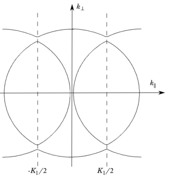
In the more general case where the potential varies periodically in all three dimensions, exactly the same arguments apply, provided that the potential coefficients are small, (that is VG << h2⏐G2⏐/8
m)
. Where the spheres centered on the different lattice points
K and
K–
G intersect, the effect of the potential is to cause the kind of remapping shown in
Figure 3-2 and
Figure 3-3 — where the two surfaces intersect it splits apart instead. The nearly free electron energy surfaces can therefore be constructed by drawing spheres of equal radius centered on each lattice point
K and rejoining them in this manner where they intersect, to form a set of nonintersecting surfaces. Although this procedure sounds simple, in practice rather complicated energy surfaces result from the procedure.
Ref. 2 considers the example of a simple cubic material in detail, and
Ref. 1 shows several examples of constant energy surfaces for different lattices.
Considering the approximations made in deriving the nearly free electron model, it is quite remarkable that the model agrees so well with the measured
Ek surfaces of many real materials, particularly considering that the true potential is expected to vary rapidly in the vicinity of the atomic cores. The reason for the success of the nearly free electron theory is related to many-body effects. In materials where it is possible to divide the electrons into tightly bound core electrons and weakly bound valence electrons, the core electrons and the ions can be replaced by a pseudo-ion with a weakly varying pseudopotential, surrounded by the outermost valence electrons. The wave function for the valence states must be orthogonal to that of the core states and the pseudopotential is constructed to ensure that this is the case. The resulting potential varies much more slowly than the true potential as a result of a
Pauli repulsion effect. This effect repels the valence electrons away from the core states in order to ensure that the corresponding wave functions are orthogonal. The nearly free electron model can then be applied to real materials if the pseudopotential, rather than the true potential, is used.
To compute the density of states in k-space the periodic boundary condition is applied, in this case on a crystal made up of Nc = N1× N2× N3 unit cells in the
a1,
a2,
and
a3 directions. Using the periodic boundary condition for the wave function gives the equation:
Equation 3-13 adds the additional requirements:
where n1,
n2,
and
n3 are integers. The reciprocal space volume per allowed
k-vector is given by:
where ξBZ is the volume of the Brillouin zone in
k-space. Consequently, the number of allowed wave vectors in a single Brillouin zone is equal to the number of unit cells in the crystal. Since each state can accommodate two electrons of opposite spin, filling one band over the entire Brillouin zone corresponds to a crystal with two valence electrons per unit cell. The density of states in
k-space is given by:
(3-19)

where the volume of the Brillouin zone (ξBZ=8
π3/
Ωu where
Ωu is the unit cell volume) has been calculated explicitly using
Equation 3-10 and vector algebra (note also that
Ω = NcΩu is the volume of the crystal itself). This result is identical to that obtained by the Sommerfeld model.
The available states in the crystal are filled up in the same way as in the Sommerfeld model. The occupancy of the states is still given by Equation 3-5 and the
Fermi level is defined by
Equation 3-6. For a metal, the Fermi surface geometry in a periodic potential reflects the equipotential surfaces of the band structure at the Fermi energy (for example in the previous section surfaces like those shown in
Figure 3-3). In semiconductors and insulators the Fermi energy lies within the band gap so there is no clear Fermi surface. However, in semiconductors the Fermi function slightly overlaps the band above (below) the Fermi level, known as the
conduction band (or the
valence band), and the states near the bottom (top) of the band have a low but significant probability of being occupied (unoccupied). Since it is these states that lead to the conductivity of semiconductors (see
The Semiclassical Model), it is worth considering what form the density of states takes at the very edge of a band.
(3-20)

Here the constants m∗x,
m∗y,
and
m∗z are associated with the
k′x,
k′y, and
k′z terms in the series, respectively. The reason for choosing this form of the (arbitrary) constant becomes apparent below. The coordinate system for the vectors
k′ has its origin at the minimum of the band in
k-space and is aligned so that
Equation 3-20 applies in the form given. There are no first-order terms in the expansion since it is at a minimum in the E(
k') relationship (that is, it is at the bottom of a band), which represents the equation of an ellipsoidal surface. Close to the band edge the constant energy surfaces are therefore ellipsoids, with a semi-axis in the
k′x direction given by
and similarly for the k′y and
k′z directions. A given constant energy surface contains a volume given by
(3-21)

This result is identical in form to Equation 3-7, except that the mass has been replaced by an effective mass,
m*=(
m∗x m∗y m∗z)
1/3 (the constants in
Equation 3-20 are named in a manner consistent with this result).
(3-22)

At this point it is useful to consider an alternative representation of the wave function, known as the Wannier function. Wannier functions,
Wn(
r − R), are wave packets of Bloch functions (
Ψnk(
r)) that are localized at a particular lattice vector
R. These are defined in the following way:
(3-23)

where N is the number of unit cells in the crystal. The Wannier functions are orthogonal since:
(3-24)

The band structure of silicon is illustrated in Figure 3-4. Although the three-dimensional band structure is considerably more complex than the simple picture described, many of the principles described are appropriate. Silicon is an indirect band-gap semiconductor, which means that the bottom of the conduction bands occur at a different point in k-space to the top of the valence bands. The valence band maxima occur at the center of the Brillouin zone. The conduction band minima occur at approximately 4/5 of the distance from the zone center to its edge along the
kx,
ky, and
kz axes.
Considering first the conduction bands, there are six symmetry equivalent minima in the locations shown in Figure 3-4. Physically the form of the energy density of states is important to determine the transport properties of the semiconductor. All six of the conduction band minima are equivalent and consequently the contributions to the density of states can be added. The constant energy surfaces near the band minima are close to being ellipsoidal;
Equation 3-21 gives a good description of the energy density of states. The transport properties of the band can be characterized by a single effective mass without any loss of accuracy in the model.
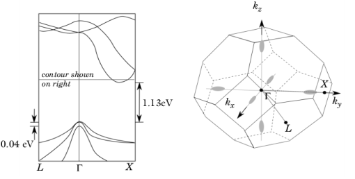
There are two coincident valence band maxima located at point Γ. An additional valence band, with a slightly lower maximum energy (produced by spin-orbit coupling, see
Ref. 1) is also located at this point. Each of these bands has a different effective mass associated with it. It is common to represent the effect of the three valence bands with an average density of states so that
Equation 3-22 is assumed. Strictly speaking this assumption is less accurate for holes than it is for electrons, as a result of the different energies associated with the band minima.