PDF

Solid Multilayer Shell Comparison
Introduction
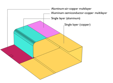
This example is a benchmark test showing that the Electric Currents in Layered Shells physics interface gives results equivalent to those from a model using the Electric Currents interface based on a solid 3D representation. Figure 1 shows the solid representation of the model geometry where an aluminum shell and a copper shell are connected through a thin semiconductor layer.
The model solves for the structure both on the true solid representation as shown in Figure 1, and on the approximative shell representation in Figure 2. The shell description is simpler from the geometrical drawing and meshing perspectives, but requires specialized features that offer the option to couple different layer materials properly. A mix of several geometrical junctions and feedings, together with also showing the full 3D equivalent, makes this model suitable as an introduction to the Electric Currents in Layered Shells interface.
Figure 1: The solid representation of the model.
Figure 2: The shell representation of the model.
Model Definition
The model contains a planar, 0.1 mm thick, semiconductor layer embedded between two thicker complex-shaped metallic profiles. The lower layer is made of copper, while the upper layer is made of aluminum. A current is applied on a square terminal on the upper surface of the aluminum layer, while ground is placed on a lateral surface of the copper. The electrical conductivity of the semiconductor is 1000 S/m, that is considerably lower than that of the connecting metal layers. The aim is to compute and compare the electric potential distribution in the various layers, both for the solid representation and for the layered shell approach.
Modeling approach
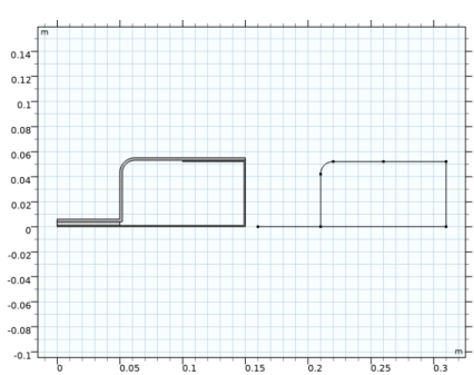
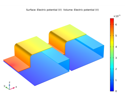
For easy comparison, the model is solved with Electric Currents interface and the Electric Currents in Layered Shells interface applied on separate objects in the same geometry as shown in figure 3 and 4. In these figures, the solid representation is on the left side, while the shell representation is on the right side.
Figure 3: Side view of solid and shell geometric configurations.
Figure 4: 3D view of solid and shell geometric configurations.
Solid modeling is, from the physics point of view, the standard choice and usually the most accurate approach. It is featured in many applications including the Introduction to COMSOL Multiphysics manual. The only special thing here is that, in the solid representation, the thin semiconductor layer is meshed using a swept mesh. The geometry for the layered shell model does not require any particular attention and a free surface triangular mesh is used.
On the accuracy of using the Electric Currents in layered Shells interface
The Electric Currents in Layered Shells interface represents the shell through boundaries by taking care of the details inside the shell (each Layered Material domain contains an underlying extra dimension where the volumetric 3D physics is represented). By setting the Shell Properties ‘From material’ and checking ‘Use all layers’, the properties of the shell can be automatically detected. Wherever the Layered Material is applied (magenta and red regions in Figure 2) both perpendicular and tangential currents are fully taken into account. Wherever Single Layer Material or other material with Shell property are applied (yellow and cyan regions in Figure 2) only tangential currents are accounted for and the electric potential will be constant in the direction normal to the shell. This is physically consistent with the single layer where the current is almost exclusively tangential. The limitation of the accuracy of the shell model is then essentially within the approximation of the geometrical representation of the shell midplane and the expected discrepancy of solid versus shell models is within the order of the ratio of thickness to length. This means the thinner the shell is, the more accurate the shell model will be, in respect to the exact solution. It is however worth noting that the Electric Currents in Layered Shells interface offers features which make it possible to simulate objects which are so thin that a 3D volumetric representation would very cumbersome or expensive due to meshing difficulties.
Results and Discussion
The model is solved in a stationary study. A solid/volumetric representation of the surface electric potential in the solid and shell objects is plotted in Figure 5. A special dataset enables the user to represent the shell with its appropriate physical thickness and offset.
Figure 5: Electric potential on the solid (left) and on the shell description (right).
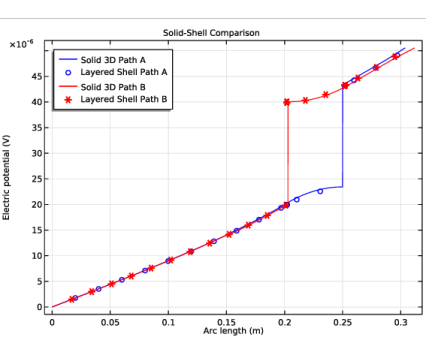
For a more quantitative comparison, in Figure 6, the electric potential is plotted along inner (blue) and outer (red) edge profiles for the solid description (solid line) and for the shell description (symbols). The comparison shows good agreement between the 3D solid model and the layered shell model. Note that the results compare well also in the region where the blue and red lines differ substantially. This region has a significant potential drop in the normal direction that is introduced by the thin semiconductor layer. The agreement among curves and symbols in the potential drop between red and blue data sets implies that the layered shell model resolves the current perpendicular to the semiconductor layer. The agreement in the potential drop from left to right indicates that the tangential currents are properly solved too. To conclude, this benchmark example showcases the ability of the layered shell interface to describe 3D currents in generic resistive and conductive layered structures.
Figure 6: Comparison of the simulated electric potential along Path A and B for the solid and shell description, where the definitions of Path A and B are given in the section Modeling Instructions — Solid-Shell Comparison.
Application Library path: ACDC_Module/Layered_Shell/solid_multilayer_shell_comparison
Modeling Instructions
From the File menu, choose New.
New
In the New window, click Model Wizard.
Model Wizard
1
In the Model Wizard window, click 3D.
2
In the Select Physics tree, select AC/DC>Electric Fields and Currents>Electric Currents (ec).
3
Click Add.
4
In the Select Physics tree, select AC/DC>Electric Fields and Currents>Electric Currents in Layered Shells (ecis).
5
Click Add.
6
Click Study.
7
In the Select Study tree, select General Studies>Stationary.
8
Click Done.
Global Definitions
Parameters 1
1
In the Model Builder window, under Global Definitions click Parameters 1.
2
In the Settings window for Parameters, locate the Parameters section.
3
Add Material
1
In the Home toolbar, click Add Material to open the Add Material window.
2
Go to the Add Material window.
3
4
Click Add to Global Materials.
5
In the tree, select Built-in>Aluminum.
6
Click Add to Global Materials.
7
In the tree, select Built-in>Copper.
8
Click Add to Global Materials.
9
In the Home toolbar, click Add Material to close the Add Material window.
Global Definitions
Material 4 (mat4)
1
In the Model Builder window, under Global Definitions right-click Materials and choose Blank Material.
2
In the Settings window for Material, type Semiconductive Material in the Label text field.
3
Click to expand the Material Properties section. In the Material properties tree, select Basic Properties>Electrical Conductivity.
4
Click Add to Material.
5
In the Material properties tree, select Basic Properties>Relative Permittivity.
6
Click Add to Material.
7
Locate the Material Contents section. In the table, enter the following settings:
Layered Material 1 (lmat1)
1
Right-click Materials and choose Layered Material.
2
In the Settings window for Layered Material, type Al-Air-Cu Stack in the Label text field.
3
Locate the Layer Definition section. Click Add.
4
Click Add.
5
Layered Material 2 (lmat2)
1
Right-click Materials and choose Layered Material.
2
In the Settings window for Layered Material, type Cu-Semi-Al Stack in the Label text field.
3
Locate the Layer Definition section. Click Add.
4
Click Add.
5
Geometry 1
Work Plane 1 (wp1)
1
In the Geometry toolbar, click Work Plane.
2
In the Settings window for Work Plane, locate the Plane Definition section.
3
From the Plane list, choose xz-plane.
4
Click Show Work Plane.
Work Plane 1 (wp1)>Rectangle 1 (r1)
1
In the Work Plane toolbar, click Rectangle.
2
In the Settings window for Rectangle, locate the Size and Shape section.
3
In the Width text field, type 0.15.
4
In the Height text field, type Cu_thickness.
Work Plane 1 (wp1)>Rectangle 2 (r2)
1
Right-click Component 1 (comp1)>Geometry 1>Work Plane 1 (wp1)>Plane Geometry>Rectangle 1 (r1) and choose Duplicate.
2
In the Settings window for Rectangle, locate the Size and Shape section.
3
In the Width text field, type 0.05.
4
In the Height text field, type Air_thickness.
5
Locate the Position section. In the yw text field, type Cu_thickness.
Work Plane 1 (wp1)>Rectangle 3 (r3)
1
Right-click Component 1 (comp1)>Geometry 1>Work Plane 1 (wp1)>Plane Geometry>Rectangle 2 (r2) and choose Duplicate.
2
In the Settings window for Rectangle, locate the Size and Shape section.
3
In the Height text field, type Al_thickness.
4
Locate the Position section. In the yw text field, type Cu_thickness+Air_thickness.
Work Plane 1 (wp1)>Rectangle 4 (r4)
1
Right-click Component 1 (comp1)>Geometry 1>Work Plane 1 (wp1)>Plane Geometry>Rectangle 3 (r3) and choose Duplicate.
2
In the Settings window for Rectangle, locate the Size and Shape section.
3
In the Width text field, type Al_thickness.
4
In the Height text field, type 0.055-Cu_thickness-Air_thickness.
5
Locate the Position section. In the xw text field, type 0.05.
Work Plane 1 (wp1)>Rectangle 5 (r5)
1
Right-click Component 1 (comp1)>Geometry 1>Work Plane 1 (wp1)>Plane Geometry>Rectangle 4 (r4) and choose Duplicate.
2
In the Settings window for Rectangle, locate the Size and Shape section.
3
In the Width text field, type Cu_thickness.
4
In the Height text field, type 0.055-2*Cu_thickness-Al_thickness.
5
Locate the Position section. In the xw text field, type 0.15-Cu_thickness.
6
In the yw text field, type Cu_thickness.
Work Plane 1 (wp1)>Rectangle 6 (r6)
1
Right-click Component 1 (comp1)>Geometry 1>Work Plane 1 (wp1)>Plane Geometry>Rectangle 5 (r5) and choose Duplicate.
2
In the Settings window for Rectangle, locate the Size and Shape section.
3
In the Width text field, type 0.1-Al_thickness.
4
In the Height text field, type Al_thickness.
5
Locate the Position section. In the xw text field, type 0.05+Al_thickness.
6
In the yw text field, type 0.055-Al_thickness.
Work Plane 1 (wp1)>Rectangle 7 (r7)
1
Right-click Component 1 (comp1)>Geometry 1>Work Plane 1 (wp1)>Plane Geometry>Rectangle 6 (r6) and choose Duplicate.
2
In the Settings window for Rectangle, locate the Size and Shape section.
3
In the Width text field, type 0.05.
4
In the Height text field, type Cu_thickness.
5
Locate the Position section. In the xw text field, type 0.1.
6
In the yw text field, type 0.055-Al_thickness-Cu_thickness.
Work Plane 1 (wp1)>Rectangle 8 (r8)
1
Right-click Component 1 (comp1)>Geometry 1>Work Plane 1 (wp1)>Plane Geometry>Rectangle 7 (r7) and choose Duplicate.
2
In the Settings window for Rectangle, locate the Size and Shape section.
3
In the Height text field, type Semi_thickness.
4
Locate the Position section. In the yw text field, type 0.055-Al_thickness-Semi_thickness.
5
In the Work Plane toolbar, click Build All.
6
Click the Zoom Extents button in the Graphics toolbar.
Work Plane 1 (wp1)>Union 1 (uni1)
1
In the Work Plane toolbar, click Booleans and Partitions and choose Union.
2
Select the objects r3, r4, and r6 only.
3
In the Settings window for Union, locate the Union section.
4
Clear the Keep interior boundaries check box.
Work Plane 1 (wp1)>Union 2 (uni2)
1
In the Work Plane toolbar, click Booleans and Partitions and choose Union.
2
Select the objects r1, r5, and r7 only.
3
In the Settings window for Union, locate the Union section.
4
Clear the Keep interior boundaries check box.
5
In the Work Plane toolbar, click Build All.
6
Click the Zoom Extents button in the Graphics toolbar.
Work Plane 1 (wp1)>Delete Entities 1 (del1)
1
In the Model Builder window, right-click Plane Geometry and choose Delete Entities.
2
On the object uni1, select Boundaries 6 and 9 only.
3
In the Settings window for Delete Entities, click Build Selected.
4
Click the Zoom Extents button in the Graphics toolbar.
Work Plane 1 (wp1)>Line Segment 1 (ls1)
1
In the Work Plane toolbar, click More Primitives and choose Line Segment.
2
In the Settings window for Line Segment, locate the Starting Point section.
3
From the Specify list, choose Coordinates.
4
Locate the Endpoint section. From the Specify list, choose Coordinates.
5
Locate the Starting Point section. In the xw text field, type 0.05.
6
Locate the Endpoint section. In the xw text field, type 0.15.
7
Locate the Starting Point section. In the yw text field, type 0.055.
8
Locate the Endpoint section. In the yw text field, type 0.055.
Work Plane 1 (wp1)>Convert to Solid 1 (csol1)
1
In the Work Plane toolbar, click Conversions and choose Convert to Solid.
2
Select the objects del1 and ls1 only.
3
In the Settings window for Convert to Solid, click Build Selected.
Work Plane 1 (wp1)>Polygon 1 (pol1)
1
In the Work Plane toolbar, click Polygon.
2
In the Settings window for Polygon, locate the Object Type section.
3
From the Type list, choose Open curve.
4
Locate the Coordinates section. From the Data source list, choose Vectors.
5
In the xw text field, type 0.16 0.31 0.31 0.31 0.31 0.26 0.26 0.26 0.21 0.21 0.21.
6
In the yw text field, type 0 0 0 0.052 0.052 0.052 0.052 0.052 0.052 0 0.
7
In the Work Plane toolbar, click Build All.
8
Click the Zoom Extents button in the Graphics toolbar.
Work Plane 1 (wp1)>Fillet 1 (fil1)
1
In the Work Plane toolbar, click Fillet.
2
On the object csol1, select Point 7 only.
3
In the Settings window for Fillet, locate the Radius section.
4
In the Radius text field, type 0.01.
5
Click Build Selected.
Work Plane 1 (wp1)>Fillet 2 (fil2)
1
In the Work Plane toolbar, click Fillet.
2
On the object fil1, select Point 5 only.
3
In the Settings window for Fillet, locate the Radius section.
4
In the Radius text field, type 0.01+Al_thickness.
5
Click Build Selected.
Work Plane 1 (wp1)>Fillet 3 (fil3)
1
In the Work Plane toolbar, click Fillet.
2
Click the Zoom Extents button in the Graphics toolbar.
3
On the object pol1, select Point 3 only.
4
In the Settings window for Fillet, locate the Radius section.
5
In the Radius text field, type 0.01.
6
Click Build Selected.
Work Plane 1 (wp1)
In the Model Builder window, click Work Plane 1 (wp1).
Extrude 1 (ext1)
1
In the Geometry toolbar, click Extrude.
2
In the Settings window for Extrude, locate the Distances section.
3
4
Click the Zoom Extents button in the Graphics toolbar.
5
Click Build Selected.
Work Plane 1 (wp1)
In the Model Builder window, collapse the Component 1 (comp1)>Geometry 1>Work Plane 1 (wp1) node.
Delete Entities 1 (del1)
1
In the Model Builder window, right-click Geometry 1 and choose Delete Entities.
2
In the Settings window for Delete Entities, locate the Entities or Objects to Delete section.
3
From the Geometric entity level list, choose Domain.
4
On the object ext1, select Domains 2, 3, and 7 only.
5
Click Build Selected.
Delete Entities 2 (del2)
1
Right-click Geometry 1 and choose Delete Entities.
2
On the object del1, select Boundaries 50, 52, and 56 only.
3
In the Settings window for Delete Entities, click Build Selected.
Work Plane 2 (wp2)
1
In the Geometry toolbar, click Work Plane.
2
In the Settings window for Work Plane, locate the Plane Definition section.
3
From the Plane type list, choose Face parallel.
4
On the object del2, select Boundary 14 only.
Plane Geometry
In the Model Builder window, click Plane Geometry.
Work Plane 2 (wp2)>Rectangle 1 (r1)
1
In the Work Plane toolbar, click Rectangle.
2
In the Settings window for Rectangle, locate the Size and Shape section.
3
In the Width text field, type 0.01.
4
In the Height text field, type 0.01.
5
Locate the Position section. In the xw text field, type -0.025.
6
In the yw text field, type -0.005.
Work Plane 2 (wp2)
1
In the Model Builder window, click Work Plane 2 (wp2).
2
In the Settings window for Work Plane, locate the Selections of Resulting Entities section.
3
Select the Resulting objects selection check box.
4
In the Label text field, type Feeding surface in Volumetric Geometry.
5
Click Build Selected.
Copy 1 (copy1)
1
In the Geometry toolbar, click Transforms and choose Copy.
2
3
In the Settings window for Copy, locate the Displacement section.
4
In the x text field, type 0.16.
5
In the z text field, type -Cu_thickness-Air_thickness-Al_thickness.
6
In the Label text field, type Feeding surface in Shell Geometry.
7
Locate the Selections of Resulting Entities section. Select the Resulting objects selection check box.
8
Click Build All Objects.
9
Click the Zoom Extents button in the Graphics toolbar.
Materials
Material Link 1 (matlnk1)
1
In the Model Builder window, under Component 1 (comp1) right-click Materials and choose More>Material Link.
2
In the Settings window for Material Link, type Solid: Air in the Label text field.
3
Material Link 2 (matlnk2)
1
Right-click Materials and choose More>Material Link.
2
In the Settings window for Material Link, type Solid: Aluminum in the Label text field.
3
Locate the Link Settings section. From the Material list, choose Aluminum (mat2).
4
Material Link 3 (matlnk3)
1
Right-click Materials and choose More>Material Link.
2
In the Settings window for Material Link, type Solid: Copper in the Label text field.
3
Locate the Link Settings section. From the Material list, choose Copper (mat3).
4
Material Link 4 (matlnk4)
1
Right-click Materials and choose More>Material Link.
2
In the Settings window for Material Link, type Solid: Semiconductive Material in the Label text field.
3
Locate the Link Settings section. From the Material list, choose Semiconductive Material (mat4).
4
Layered Material Link 1 (llmat1)
1
Right-click Materials and choose Layers>Layered Material Link.
2
In the Settings window for Layered Material Link, type Shell: Al-Air-Cu in the Label text field.
3
4
Locate the Orientation and Position section. From the Position list, choose User defined.
5
In the Relative midplane offset text field, type -(Cu_thickness+Air_thickness)/(Cu_thickness+Air_thickness+Al_thickness).
In a COMSOL geometry, all boundaries are equipped with a surface normal. The surface normal is a unit vector that is tied to what is considered the upside and downside of the boundary. For layered materials, the normal vector dictates the direction in which the layers are stacked. When an offset is specified, the layer stack is shifted in the direction of the surface normal. Although the shift will not affect the solution (as curvature is neglected), it does affect how the layers are displayed in postprocessing.
Layered Material Link 2 (llmat2)
1
Right-click Materials and choose Layers>Layered Material Link.
2
In the Settings window for Layered Material Link, type Shell: Cu-Semi-Al in the Label text field.
3
Locate the Layered Material Settings section. From the Material list, choose Cu-Semi-Al Stack (lmat2).
4
5
Locate the Orientation and Position section. From the Position list, choose Downside on boundary.
6
In the Home toolbar, click Windows and choose Add Material from Library.
Add Material
1
Go to the Add Material window.
2
In the tree, select Built-in>Aluminum and Built-in>Copper.
3
Click Add to Component 1 (comp1).
Materials
Aluminum (mat5)
1
In the Model Builder window, under Component 1 (comp1)>Materials click Aluminum (mat5).
2
In the Settings window for Material, locate the Geometric Entity Selection section.
3
From the Geometric entity level list, choose Boundary.
4
Click to expand the Material Properties section. In the Material properties tree, select Geometric Properties>Shell.
5
Click Add to Material.
6
In the Model Builder window, expand the Aluminum (mat5) node, then click Shell (shell).
7
In the Settings window for Property Group, locate the Layer Definition section.
8
In the Thickness text field, type Al_thickness.
9
In the Model Builder window, click Aluminum (mat5).
10
In the Settings window for Material, type Shell: Al in the Label text field.
11
12
Locate the Orientation and Position section. From the Position list, choose User defined.
13
In the Relative midplane offset text field, type 1+2*(Semi_thickness+Cu_thickness)/Al_thickness.
Copper (mat6)
1
In the Model Builder window, click Copper (mat6).
2
In the Settings window for Material, locate the Geometric Entity Selection section.
3
From the Geometric entity level list, choose Boundary.
4
Click to expand the Material Properties section. In the Material properties tree, select Geometric Properties>Shell.
5
Click Add to Material.
6
In the Model Builder window, expand the Copper (mat6) node, then click Shell (shell).
7
In the Settings window for Property Group, locate the Layer Definition section.
8
In the Thickness text field, type Cu_thickness.
9
In the Model Builder window, click Copper (mat6).
10
In the Settings window for Material, type Shell: Cu in the Label text field.
11
12
Locate the Orientation and Position section. From the Position list, choose Downside on boundary.
Electric Currents (ec)
1
In the Model Builder window, under Component 1 (comp1) click Electric Currents (ec).
2
In the Settings window for Electric Currents, locate the Domain Selection section.
3
4
Click Remove from Selection.
5
Ground 1
1
In the Physics toolbar, click Boundaries and choose Ground.
2
Click the Zoom Extents button in the Graphics toolbar.
3
4
Click the Zoom Extents button in the Graphics toolbar.
Terminal 1
1
In the Physics toolbar, click Boundaries and choose Terminal.
2
In the Settings window for Terminal, locate the Terminal section.
3
In the I0 text field, type 1.
4
5
Click the Zoom Extents button in the Graphics toolbar.
Electric Currents in Layered Shells (ecis)
1
In the Model Builder window, under Component 1 (comp1) click Electric Currents in Layered Shells (ecis).
2
In the Settings window for Electric Currents in Layered Shells, locate the Boundary Selection section.
3
Select the Restrict to layered boundaries check box.
Conductive Shell 1
In the Model Builder window, expand the Component 1 (comp1)>Electric Currents in Layered Shells (ecis)>Conductive Shell 1 node, then click Conductive Shell 1.
Terminal 1
1
In the Physics toolbar, click Attributes and choose Terminal.
2
In the Settings window for Terminal, locate the Boundary Selection section.
3
From the Selection list, choose Manual.
4
5
Locate the Interface Selection section. From the Apply to list, choose Bottom interface.
6
Locate the Terminal section. In the I0 text field, type 1.
Ground 1
1
In the Physics toolbar, click Edges and choose Ground.
2
3
In the Settings window for Ground, locate the Shell Properties section.
4
Clear the Use all layers check box.
5
Specify the Selection vector as
Ground 2
1
In the Physics toolbar, click Edges and choose Ground.
2
Continuity 1
1
In the Physics toolbar, click Edges and choose Continuity.
2
In the Settings window for Continuity, locate the Layer Selection section.
3
From the Source list, choose Shell: Al-Air-Cu (llmat1)-[lmat1].
4
From the Destination list, choose Shell: Al (mat5).
Continuity 2
1
In the Physics toolbar, click Edges and choose Continuity.
2
In the Settings window for Continuity, locate the Layer Selection section.
3
From the Source list, choose Shell: Al-Air-Cu (llmat1)-[lmat1].
4
From the Destination list, choose Shell: Cu (mat6).
5
In the Selection table, enter the following settings:
Continuity 3
1
In the Physics toolbar, click Edges and choose Continuity.
2
In the Settings window for Continuity, locate the Layer Selection section.
3
From the Source list, choose Shell: Cu-Semi-Al (llmat2)-[lmat2].
4
From the Destination list, choose Shell: Al (mat5).
5
In the Selection table, enter the following settings:
Continuity 4
1
In the Physics toolbar, click Edges and choose Continuity.
2
In the Settings window for Continuity, locate the Layer Selection section.
3
From the Source list, choose Shell: Cu-Semi-Al (llmat2)-[lmat2].
4
From the Destination list, choose Shell: Cu (mat6).
Insulating Layer 1
1
In the Physics toolbar, click Boundaries and choose Insulating Layer.
2
In the Settings window for Insulating Layer, locate the Boundary Selection section.
3
From the Selection list, choose All boundaries.
4
Locate the Shell Properties section. Specify the Selection vector as
Mesh 1
Free Tetrahedral 1
1
In the Model Builder window, under Component 1 (comp1) right-click Mesh 1 and choose Free Tetrahedral.
2
In the Settings window for Free Tetrahedral, locate the Domain Selection section.
3
From the Geometric entity level list, choose Domain.
4
5
Click Build Selected.
Swept 1
1
In the Model Builder window, right-click Mesh 1 and choose Swept.
2
In the Settings window for Swept, locate the Domain Selection section.
3
From the Geometric entity level list, choose Domain.
4
5
Click Build Selected.
Free Tetrahedral 2
1
Right-click Mesh 1 and choose Free Tetrahedral.
2
In the Settings window for Free Tetrahedral, locate the Domain Selection section.
3
From the Geometric entity level list, choose Domain.
4
5
Click the Zoom Extents button in the Graphics toolbar.
6
Click Build Selected.
7
Click the Zoom Extents button in the Graphics toolbar.
Free Triangular 1
1
Right-click Mesh 1 and choose More Operations>Free Triangular.
2
Size 1
1
Right-click Free Triangular 1 and choose Size.
2
In the Settings window for Size, locate the Element Size section.
3
Click the Custom button.
4
Locate the Element Size Parameters section. Select the Maximum element size check box.
5
Select the Minimum element size check box.
6
In the Maximum element size text field, type 0.005.
7
In the Minimum element size text field, type 0.005.
8
Click Build All.
For the solid representation, there is one unique expression for the electric potential: <c>V</c>. For the layered shell representation however, there are several (depending on which side of the boundary you are): <c>ecis.Vup</c>, <c>ecis.Vdown</c>, and <c>ecis.Vav</c>. As certain parts of the shell geometry show material discontinuities and varying definitions of the surface normal, the appropriate expression to use in the plot differs from place to place. In order to simplify postprocessing, we define a couple of intermediate variables.
The battery charging and discharging variables are set up as follows:
For the solid representation, there is one unique expression for the electric potential: V. For the layered shell representation however, there are several (depending on which side of the boundary you are): ecis.Vup, ecis.Vdown, and ecis.Vav. As certain parts of the shell geometry show material discontinuities and varying definitions of the surface normal, the appropriate expression to use in the plot differs from place to place. In order to simplify postprocessing, we define a couple of intermediate variables.
The battery charging and discharging variables are set up as follows:
Definitions (comp1)
Variables 1
1
In the Model Builder window, under Component 1 (comp1) right-click Definitions and choose Variables.
2
In the Settings window for Variables, locate the Geometric Entity Selection section.
3
From the Geometric entity level list, choose Boundary.
4
5
Locate the Variables section. In the table, enter the following settings:
Notice that the normal of these boundaries is pointed down (in the minus z direction).
Variables 2
1
Right-click Definitions and choose Variables.
2
In the Settings window for Variables, locate the Geometric Entity Selection section.
3
From the Geometric entity level list, choose Boundary.
4
5
Locate the Variables section. In the table, enter the following settings:
Variables 3
1
Right-click Definitions and choose Variables.
2
In the Settings window for Variables, locate the Geometric Entity Selection section.
3
From the Geometric entity level list, choose Boundary.
4
5
Locate the Variables section. In the table, enter the following settings:
Variables 4
1
Right-click Definitions and choose Variables.
2
In the Settings window for Variables, locate the Geometric Entity Selection section.
3
From the Geometric entity level list, choose Boundary.
4
5
Locate the Variables section. In the table, enter the following settings:
Study 1
In the Home toolbar, click Compute.
Results
Multislice 1
1
In the Model Builder window, expand the Electric Potential (ec) node, then click Multislice 1.
2
In the Settings window for Multislice, locate the Multiplane Data section.
3
Find the Y-planes subsection. In the Planes text field, type 18.
4
In the Electric Potential (ec) toolbar, click Plot.
Electric Potential (ecis)
1
In the Model Builder window, click Electric Potential (ecis).
2
In the Settings window for 3D Plot Group, locate the Plot Settings section.
3
Clear the Plot dataset edges check box.
The default plot Electric Potential (ecis) shows the electric potential in the shell. In addition to this, add the electric potential in the solid.
Volume 1
1
Right-click Electric Potential (ecis) and choose Volume.
2
In the Settings window for Volume, type Solid Electric Potential in the Label text field.
3
Locate the Data section. From the Dataset list, choose Study 1/Solution 1 (sol1).
4
Click to expand the Inherit Style section. From the Plot list, choose Surface 1.
5
Click the Show Grid button in the Graphics toolbar.
6
In the Electric Potential (ecis) toolbar, click Plot.
Modeling Instructions — Solid-Shell Comparison
In the following part, we create a plot for the electric potential along a set of selected paths for both the solid and the shell description. Start by defining the edges used for the comparison.
Definitions (comp1)
Explicit 1
1
In the Definitions toolbar, click Explicit.
2
In the Settings window for Explicit, type Solid Path A in the Label text field.
3
Locate the Input Entities section. From the Geometric entity level list, choose Edge.
4
5
Click the Zoom to Selection button in the Graphics toolbar.
6
Click the Wireframe Rendering button in the Graphics toolbar.
7
Click the Zoom Extents button in the Graphics toolbar.
Explicit 2
1
In the Definitions toolbar, click Explicit.
2
In the Settings window for Explicit, type Solid Path B in the Label text field.
3
Locate the Input Entities section. From the Geometric entity level list, choose Edge.
4
5
Click the Zoom to Selection button in the Graphics toolbar.
6
Click the Zoom Extents button in the Graphics toolbar.
Explicit 3
1
In the Definitions toolbar, click Explicit.
2
In the Settings window for Explicit, type Shell Path A-B in the Label text field.
3
Locate the Input Entities section. From the Geometric entity level list, choose Edge.
4
5
Click the Zoom to Selection button in the Graphics toolbar.
Next, add the layered shell variables for path A and path B. They are entered in the same way as done for the aluminum and the copper.
Variables 1
1
In the Model Builder window, click Variables 1.
2
In the Settings window for Variables, locate the Variables section.
3
Variables 2
1
In the Model Builder window, click Variables 2.
2
In the Settings window for Variables, locate the Variables section.
3
Variables 3
1
In the Model Builder window, click Variables 3.
2
In the Settings window for Variables, locate the Variables section.
3
Variables 4
1
In the Model Builder window, click Variables 4.
2
In the Settings window for Variables, locate the Variables section.
3
Since you have introduced a couple of new variables, the solution should be updated. After that, continue by introducing the 1D plot group for the solid-shell comparison.
Study 1
In the Study toolbar, click Update Solution.
Results
1D Plot Group 3
1
In the Home toolbar, click Add Plot Group and choose 1D Plot Group.
2
In the Settings window for 1D Plot Group, type Solid-Shell Comparison in the Label text field.
3
Click to expand the Title section. From the Title type list, choose Manual.
4
In the Title text area, type Solid-Shell Comparison.
5
Locate the Plot Settings section. Select the y-axis label check box.
6
7
Locate the Legend section. From the Position list, choose Upper left.
Line Graph 1
1
Right-click Solid-Shell Comparison and choose Line Graph.
2
In the Settings window for Line Graph, locate the Selection section.
3
From the Selection list, choose Solid Path A.
4
Click to expand the Coloring and Style section. From the Color list, choose Blue.
5
Click to expand the Legends section. Select the Show legends check box.
6
From the Legends list, choose Manual.
7
Line Graph 2
1
In the Model Builder window, right-click Solid-Shell Comparison and choose Line Graph.
2
In the Settings window for Line Graph, locate the Selection section.
3
From the Selection list, choose Shell Path A-B.
4
Locate the y-Axis Data section. In the Expression text field, type V_A.
5
Locate the Coloring and Style section. From the Color list, choose Blue.
6
Find the Line style subsection. From the Line list, choose None.
7
Find the Line markers subsection. From the Marker list, choose Circle.
8
In the Number text field, type 28.
9
Locate the Legends section. Select the Show legends check box.
10
From the Legends list, choose Manual.
11
Line Graph 3
1
Right-click Solid-Shell Comparison and choose Line Graph.
2
In the Settings window for Line Graph, locate the Selection section.
3
From the Selection list, choose Solid Path B.
4
Locate the Coloring and Style section. From the Color list, choose Red.
5
Locate the Legends section. Select the Show legends check box.
6
From the Legends list, choose Manual.
7
Line Graph 4
1
Right-click Solid-Shell Comparison and choose Line Graph.
2
In the Settings window for Line Graph, locate the Selection section.
3
From the Selection list, choose Shell Path A-B.
4
Locate the y-Axis Data section. In the Expression text field, type V_B.
5
Locate the Coloring and Style section. From the Color list, choose Red.
6
Find the Line style subsection. From the Line list, choose None.
7
Find the Line markers subsection. From the Marker list, choose Asterisk.
8
In the Number text field, type 30.
9
Locate the Legends section. Select the Show legends check box.
10
From the Legends list, choose Manual.
11
Solid-Shell Comparison
The results for the solid representation and the layered shell are in agreement. Notice that this agreement requires layers that are sufficiently thin. The thinner the layer, the better the agreement.
Finally, modify the Electric Potential (ecis) plot to show a clear comparison between the solid representation and the layered shell representation.
Line 1
1
In the Model Builder window, right-click Electric Potential (ecis) and choose Line.
2
In the Settings window for Line, locate the Data section.
3
From the Dataset list, choose Study 1/Solution 1 (sol1).
4
Locate the Expression section. In the Expression text field, type 1.
5
Locate the Coloring and Style section. From the Coloring list, choose Uniform.
6
From the Color list, choose Black.
Deformation 1
1
Right-click Line 1 and choose Deformation.
2
In the Settings window for Deformation, locate the Expression section.
3
In the X component text field, type 0.
4
In the Y component text field, type 0.
5
In the Z component text field, type 0.07.
6
Locate the Scale section. Select the Scale factor check box.
7
8
Click the Go to XZ View button in the Graphics toolbar.
9
Click the Orthographic Projection button in the Graphics toolbar.
10
Click the Zoom Extents button in the Graphics toolbar.
11
In the Electric Potential (ecis) toolbar, click Plot.