Introduction
The Wave Optics Module is used by engineers and scientists to understand, predict, and design electromagnetic wave propagation and resonance effects in optical applications. Simulations of this kind result in more powerful and efficient products and engineering methods. It allows its users to quickly and accurately predict electromagnetic field distributions, transmission and reflection coefficients, and power dissipation in a proposed design. Compared to traditional prototyping, it offers the benefits of lower cost and the ability to evaluate and predict entities that are not directly measurable in experiments. It also allows the exploration of operating conditions that would destroy a real prototype or be hazardous.
This module covers electromagnetic fields and waves in two-dimensional and three-dimensional spaces. All modeling formulations are based on Maxwell’s equations together with material laws for propagation in various media. The modeling capabilities are accessed via predefined physics interfaces, collectively referred to as Wave Optics interfaces, which allow you to set up and solve electromagnetic models. The Wave Optics interfaces cover the modeling of electromagnetic fields and waves in frequency domain, time domain, eigenfrequency, and mode analysis.
Under the hood, the Wave Optics interfaces formulate and solve the differential form of Maxwell’s equations together with the initial and boundary conditions. The equations are solved using the finite element method and the boundary element method with numerically stable edge element discretization in combination with state-of-the-art algorithms for preconditioning and solution of the resulting sparse equation systems. The results are presented using predefined plots of electric and magnetic fields, reflectances, transmittances, diffraction efficiencies, S-parameters, power flow, and dissipation. You can also display your results as plots of expressions of the physical quantities that you define freely, or as tabulated derived values obtained from the simulation.
The workflow is straightforward and can be described by the following steps: define the geometry, select materials, select a suitable Wave Optics interface, define boundary and initial conditions, define the mesh, select a solver, and visualize the results. All these steps are accessed from the COMSOL Desktop. The geometry can be built from basic geometric shapes or parts, like waveguide elements, can be added from the Wave Optics Parts Library. Materials can have user-defined properties or they can be picked from any of the built-in material libraries, including the Optical Material Library. That library includes more than a thousand inorganic and organic materials, glasses, and so on. The mesh creation and solver selection steps are usually carried out automatically using default settings, which are tuned for each specific Wave Optics interface.
The Wave Optics Module application library describes the physics interfaces and their different features through tutorial and benchmark examples for the different formulations. The library includes examples addressing gratings and metamaterials, laser cavities, nonlinear optics, optical scattering, waveguides and couplers, and benchmark models for verification and validation of the Wave Optics interfaces.
This introduction is intended to give you a jump start in your modeling work. It has examples of the typical use of the Wave Optics Module, a list of the physics interfaces with a short description, and a tutorial model that introduces the modeling workflow.
The Use of the Wave Optics Module
The Wave Optics interfaces are used to model electromagnetic fields and waves in optical applications. Typical wavelengths for optical applications are in the nanometer to micrometer range, corresponding to frequencies of the order of hundreds of THz. A characteristic of optical applications is also that the structures are often much larger than the wavelength.
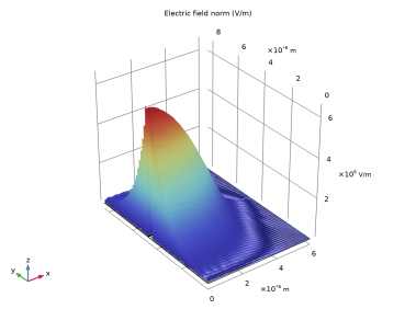
Wave Optics simulations are often used for determining propagation and coupling properties for different types of waveguide structures. Figure 1 shows the electric field distribution in a directional coupler. A wave is launched into the left waveguide. The wave couples over to the right waveguide after 2 mm propagation. The waveguides consist of ion-bombarded GaAs, surrounded by GaAs.
Figure 1: Electric field distribution in a directional coupler. Notice that the propagation length is 2 mm, whereas the cross-sectional area is 12 μm by 18 μm. From Directional Coupler in the Wave Optics Module application library.
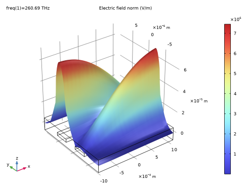
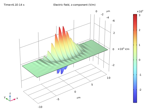
Figure 2 shows an example of transient propagation in a nonlinear crystal. The figure shows the total electric field, the sum of the incoming fundamental wave and the generated second harmonic wave, when the wave is located in the middle of the crystal.
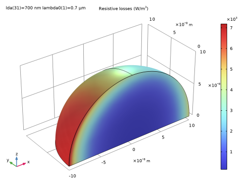
Figure 2: The z-component of the electric field after 61 fs propagation in a nonlinear crystal. From Second Harmonic Generation of a Gaussian Beam in the Wave Optics Module application library.
Transient simulations are useful for modeling nonlinear optical processes involving short optical pulses. Another example of nonlinear optical propagation is the effect of self-focusing, as shown in Figure 3. Here, the Gaussian beam and the intensity-dependent refractive index form a self-induced lens in the material that counteracts the spreading effect of diffraction.
Figure 3: The electric field distribution for a Gaussian beam propagating in a medium with an intensity-dependent refractive index. From Self-Focusing in the Wave Optics Module application library.
In Figure 4 and Figure 5, a model from the Wave Optics Module application library shows the scattering of an incoming plane wave by a small gold sphere. The model is set up using the scattered field formulation, where the incoming plane wave is entered as a background field. The scattered wave is absorbed by a Perfectly Matched Layer (PML). Figure 4 shows the volume resistive losses in the gold sphere.
Figure 4: The volume resistive losses in a small gold sphere, when excited by an incoming plane wave. From Optical Scattering Off a Gold Nanosphere in the Wave Optics Module application library.
A Far-Field Domain is used in the model to calculate the far-field pattern of the scattered waves, as shown in Figure 5.
Figure 5: The far-field radiation pattern in the E-plane (blue) and H-plane (green) when wavelength is 700 nm.
The Wave Optics Module also offers a comprehensive set of features for 2D modeling, including both source driven wave propagation and mode analysis. Figure 6 shows mode analysis of a microstructured optical fiber.
Figure 6: The surface plot visualizes the norm of the tangential and longitudinal electric and magnetic fields for one of the two degenerate HE11-like modes for a holey fiber. From Leaky Modes in a Microstructured Optical Fiber in the Wave Optics Module application library.
In both 2D and 3D, the analysis of periodic structures is popular. Figure 7 is an example of a plane wave incident on a metallic wire grating with a dielectric substrate.
Figure 7: Electric field norm for TE incidence at π/5 radians. From Plasmonic Wire Grating in the Wave Optics Module application library.
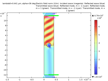
Figure 8 shows the resulting plot of the reflectances, transmittances, and diffraction efficiencies.
Figure 8: Reflectance, transmittance, and diffraction efficiencies as a function of angle of incidence. From Plasmonic Wire Grating in the Wave Optics Module application library.
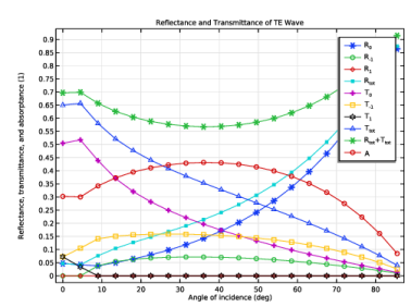
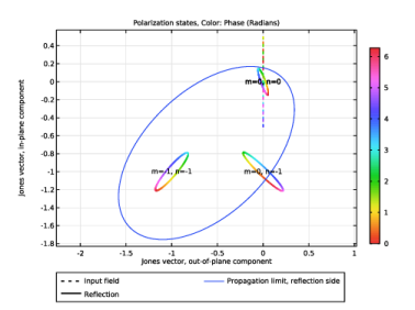
Figure 9 shows an example of a polarization plot. The polarization plot shows the state of polarization for different diffraction orders for a periodic structure. In this example, the periodic structure is a hexagonal grating.
Figure 9: Polarization state plot, showing polarization ellipses for different diffraction orders for a periodic structure. From Hexagonal Grating in the Wave Optics Module application library.
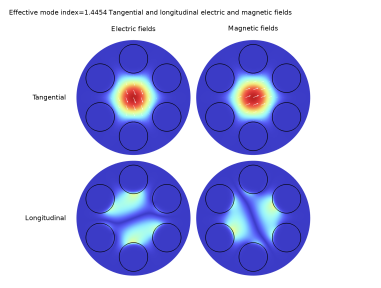
Eigenfrequency studies are of interest for photonic bandgap structure and laser cavity calculations. Figure 10 shows the mode field for a vertical-cavity surface-emitting laser (VCSEL) after a self-consistent solution for the resonance frequency and the threshold gain.
Figure 10: The mode field of a vertical-cavity surface-emitting laser (VCSEL), for a self-consistent solution of the resonance frequency and the threshold gain. From Threshold Gain Calculations for Vertical-Cavity Surface-Emitting Lasers (VCSELs) in the Wave Optics Module application library.
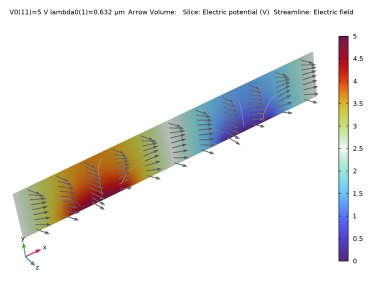
The Wave Optics interfaces can easily be combined with physics interfaces from other physics areas, such as heat transfer, structural mechanics, semiconductor physics and low-frequency electromagnetics. Figure 11 shows the result of a multiphysics simulation, combining the Electromagnetic Waves, Frequency Domain interface from the Wave Optics Module with the Electrostatics and the Weak Form PDE interfaces from the COMSOL Multiphysics platform product. Using these three physics interfaces, the Oseen–Frank equation is solved for the distribution of the directors (optical axes) in an In-Plane Switching (IPS) nematic liquid crystal cell, under an applied static electric field. The Wave Optics interface solves for the electric field for the wave, for this anisotropic and inhomogeneous liquid crystal material.
Figure 11: The director (optical axis) distribution (arrows), the electric potential (slice plot) and the static electric field (streamlines) for an in-plane switching (IPS) nematic liquid crystal cell. From In-Plane Switching of a Liquid Crystal Cell in the Wave Optics Module application library.
The Wave Optics Module has a vast range of tools to evaluate and export the results, for example, evaluation of far-field and scattering matrices (S-parameters). S-parameters can be exported in the Touchstone file format.