|
1
|
|
3
|
|
-
|
|
-
|
|
-
|
|
-
|
|
5
|
|
6
|
|
-
|
|
3
|
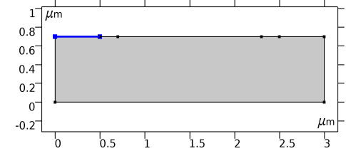
In the Settings window for Metal Contact, locate the Terminal section. In the V0 text field, type Vd.
|
|
2
|
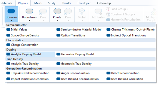
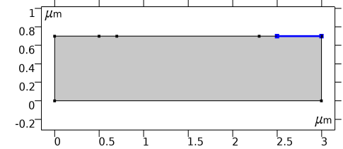
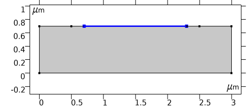
In the Settings window for Thin Insulator Gate, locate the Terminal section. In the V0 text field, type Vg.
|
|
-
|
|
-
|