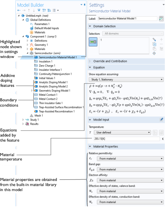
Figure 5 uses a model similar to the MOSFET application library example to show the Model Builder tree structure, and the Settings window for the selected Semiconductor Material Model 1 feature node. This node adds the semiconductor equations to the simulation within the domains selected. In the Model Inputs section the temperature of the material is specified. It is straightforward to link this temperature to a separate Heat Transfer interface to solve nonisothermal problems — the Semiconductor interface automatically defines an appropriate heat source term that can be readily accessed in a Heat Transfer interface. In the Material Properties section, the Settings window indicates that the relative permittivity and the band gap are inherited from the material properties assigned to the domain. The material properties can be set up as functions of other dependent variables in the model, for example, the temperature. The dopant density is specified by means of multiple additive doping features, which can be used to combine Gaussian and user-defined dopant density profiles to produce the desired profile. Several boundary conditions are also indicated in the model tree. The Ohmic Contact boundary condition is commonly used to model nonrectifying interconnects. The Thin Insulating Gate feature models a gate with a thickness smaller than the typical length scale of the mesh. It is also possible to model gates explicitly, solving Poisson’s equation within the dielectric.
Figure 6 shows the physics interfaces included with the Semiconductor Module. The two Semiconductor Optoelectronics interfaces are only available with an additional Wave Optics module license.
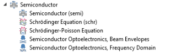
Also see Physics Interface Guide by Space Dimension and Study Type. Below, a brief overview of each of the Semiconductor Module physics interfaces is given.