
PDF

Modeling a Scatterer Near an Optical Waveguide
Introduction
The dielectric slab waveguide is one of the conceptual building blocks in photonic structure design. Although most real structures are more complex than just a two-dimensional dielectric slab, a two-dimensional model permits to simplify the analysis. This model simulates the case of a small lossy scatterer in the proximity of an optical waveguide, shows how it interacts with the fields, and calculates reflection and transmission along the waveguide, as well as losses and scattering.
Model Definition
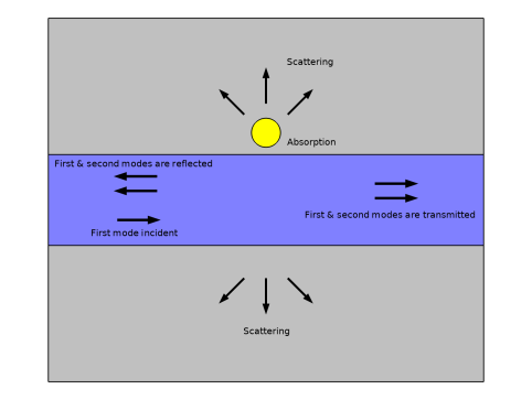
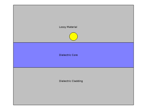
The schematic of the structure is shown in Figure 1. A dielectric slab waveguide has a small circular metallic object located nearby. The scatterer interacts with the fields, thus leading to some losses within the material, and causing scattering of light into all directions. In the absence of the nearby object, this example would reduce to a perfect dielectric slab waveguide (see the Application Library model Dielectric Slab Waveguide).
Figure 1: Schematic of a 2D dielectric slab waveguide with a lossy material in proximity to the core.
Imagine a waveguide that is wide enough to support multiple modes. For the sake of simplicity, this model restricts the analysis to just the example of the electric field polarized out of the modeling plane. Assume that either the electric or magnetic field is polarized purely out of plane and that there is no coupling between these two as long as all materials are isotropic.
Figure 2: The incident light guided along the waveguide can be reflected, transmitted, absorbed, and scattered.
The reflection and transmission along the waveguide, as well as absorption and scattering mechanisms are shown in Figure 2. Here, light propagates along the waveguide toward the scatterer (from left to right), and this incident light is the first or fundamental mode. Due to the presence of the scatterer, some fraction of the incident light will be
1
2
3
4
5
6
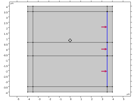
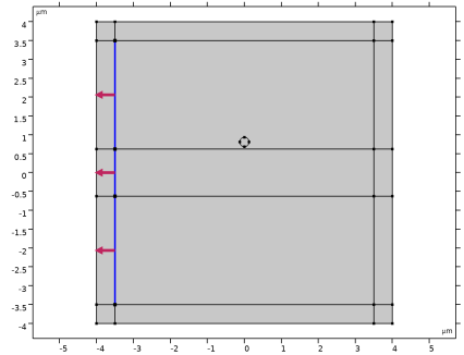
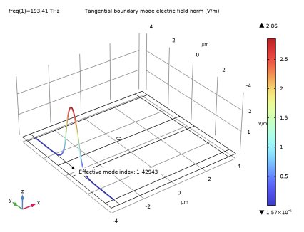
Computation of transmission into the four possible guided modes of the waveguide (items 16) requires four different numerical ports into the model, two on each side. As already discussed in Ref. 1, it is possible to introduce multiple interior slit port boundary conditions at boundaries within the modeling space. Modeling the absorption into the lossy material simply involves integrating the loss within the metallic object.
In summary, this model simulates a dielectric slab waveguide with a lossy scatterer nearby to analyze the guided light, reflection, transmission, absorption, and scattering mechanisms in 2D using the Electromagnetic Waves, Frequency Domain (ewfd) interface. Numeric ports are used and perfectly matched layers are employed to absorb most of the outgoing radiation. A Frequency Domain and four Boundary Mode Analysis study steps are applied to solve the domain fields.
Results and Discussion
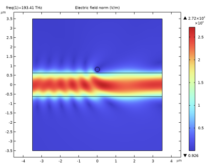
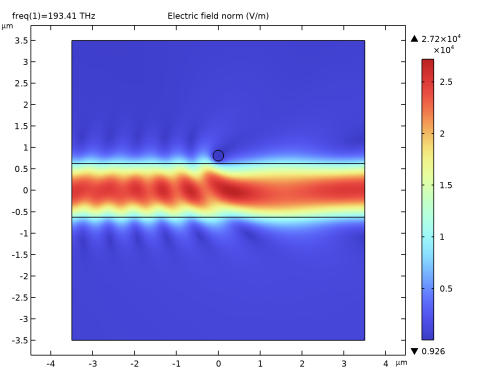
Figure 3 shows the electric field norm from the simulation. The numeric port boundary condition at the left excites a fundamental mode that propagates in the tangential direction.
Figure 3: The Electric field norm.
Figure 4 shows the total resistive losses within the scatterer. Here, the loss distribution is not uniform within the material. Maximum losses are observed at the bottom part of the scatterer which is closer to the waveguide.
Figure 4: Resistive losses in the lossy scatterer.
For further details, see the blog post in Ref. 2.
References
1. Walter Frei, “Modeling Waveguides that Support Multiple Modes,” COMSOL Blog, Aug. 12, 2020; www.comsol.com/blogs/modeling-waveguides-that-support-multiple-modes/.
2. Walter Frei, “Modeling a Scatterer Near an Optical Waveguide,” COMSOL Blog, Aug. 25, 2020; www.comsol.com/blogs/modeling-a-scatterer-near-an-optical-waveguide/.
Application Library path: Wave_Optics_Module/Waveguides/waveguide_with_scatterer
Modeling Instructions
From the File menu, choose New.
New
In the New window, click  Model Wizard.
Model Wizard
1
In the Model Wizard window, click  2D.
2
In the Select Physics tree, select Optics > Wave Optics > Electromagnetic Waves, Frequency Domain (ewfd).
3
Click Add.
4
Click  Study.
5
In the Select Study tree, select General Studies > Frequency Domain.
6
Geometry 1
1
In the Model Builder window, under Component 1 (comp1) click Geometry 1.
2
In the Settings window for Geometry, locate the Units section.
3
From the Length unit list, choose µm.
Global Definitions
Parameters 1
1
In the Model Builder window, under Global Definitions click Parameters 1.
2
In the Settings window for Parameters, locate the Parameters section.
3
Geometry 1
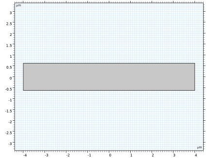
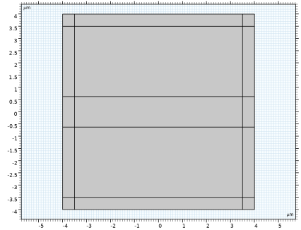
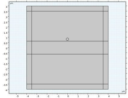
The geometry consists of a slab waveguide, with a scatterer on top, embedded in a cladding material.
Rectangle 1 (r1)
1
In the Geometry toolbar, click  Rectangle.
2
In the Settings window for Rectangle, locate the Size and Shape section.
3
In the Width text field, type L_core.
4
In the Height text field, type h_core.
5
Locate the Position section. From the Base list, choose Center.
6
Click  Build Selected.
Rectangle 2 (r2)
1
In the Geometry toolbar, click  Rectangle.
2
In the Settings window for Rectangle, locate the Size and Shape section.
3
In the Width text field, type L_core.
4
In the Height text field, type h_cladding.
5
Locate the Position section. From the Base list, choose Center.
6
Click to expand the Layers section. In the table, enter the following settings:
7
Select the Layers to the left checkbox.
8
Select the Layers to the right checkbox.
9
Select the Layers on top checkbox.
10
Click  Build Selected.
11
Click the  Zoom Extents button in the Graphics toolbar.
Circle 1 (c1)
1
In the Geometry toolbar, click  Circle.
2
In the Settings window for Circle, locate the Size and Shape section.
3
In the Radius text field, type h_core/10.
4
Locate the Position section. In the y text field, type h_core*0.65.
5
Click  Build All Objects.
Materials
Cladding
1
In the Model Builder window, under Component 1 (comp1) right-click Materials and choose Blank Material.
2
In the Settings window for Material, type Cladding in the Label text field.
3
Locate the Material Contents section. In the table, enter the following settings:
Core
1
Right-click Materials and choose Blank Material.
2
In the Settings window for Material, type Core in the Label text field.
3
4
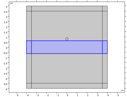
Locate the Material Contents section. In the table, enter the following settings:
Add Material
Pick gold as the lossy scatterer from the Optical material library.
1
In the Materials toolbar, click  Add Material to open the Add Material window.
2
Go to the Add Material window.
3
In the tree, select Optical > Inorganic Materials > Au - Gold > Experimental data: bulk, thick film > Au (Gold) (Johnson and Christy 1972: n,k 0.188-1.937 um).
4
Right-click and choose Add to Component 1 (comp1).
5
In the Materials toolbar, click  Add Material to close the Add Material window.
Materials
Au (Gold) (Johnson and Christy 1972: n,k 0.188-1.937 um) (mat3)
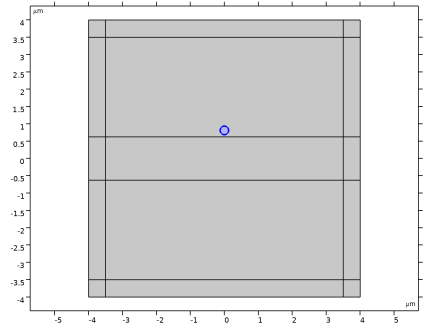
Select Domain 16 only.
Definitions
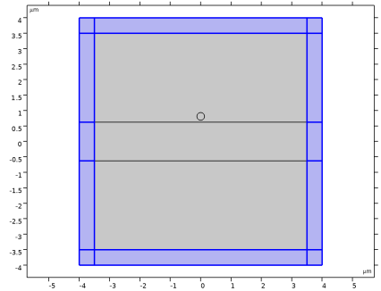
Perfectly Matched Layer 1 (pml1)
1
In the Definitions toolbar, click  Perfectly Matched Layer.
2
Electromagnetic Waves, Frequency Domain (ewfd)
Define the incident port.
1
In the Model Builder window, under Component 1 (comp1) click Electromagnetic Waves, Frequency Domain (ewfd).
2
In the Settings window for Electromagnetic Waves, Frequency Domain, locate the Components section.
3
From the Electric field components solved for list, choose Out-of-plane vector.
Port 1
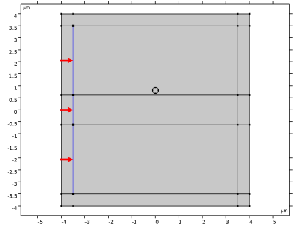
1
In the Physics toolbar, click  Boundaries and choose Port.
2
3
In the Settings window for Port, locate the Port Properties section.
4
From the Type of port list, choose Numeric.
5
In the Pin text field, type Pin.
6
Select the Activate slit condition on interior port checkbox.
7
Click Toggle Power Flow Direction.
Port 2
Define the transmission port for the first mode.
1
In the Physics toolbar, click  Boundaries and choose Port.
2
3
In the Settings window for Port, locate the Port Properties section.
4
From the Type of port list, choose Numeric.
5
Select the Activate slit condition on interior port checkbox.
Port 3
1
Right-click Port 2 and choose Duplicate.
Define the port to capture the first and second reflected modes.
2
In the Settings window for Port, locate the Boundary Selection section.
3
Click  Clear Selection.
4
5
Locate the Port Properties section. Click Toggle Power Flow Direction.
Port 4
1
Right-click Port 3 and choose Duplicate.
Define the transmission port for the second mode.
2
In the Settings window for Port, locate the Boundary Selection section.
3
Click  Clear Selection.
4
5
Locate the Port Properties section. Click Toggle Power Flow Direction. These boundaries are same as Port 2.
Mesh 1
1
In the Model Builder window, under Component 1 (comp1) click Mesh 1.
2
In the Settings window for Mesh, locate the Electromagnetic Waves, Frequency Domain (ewfd) section.
3
Select the Resolve wave in lossy media checkbox.
Study 1
Step 1: Frequency Domain
1
In the Model Builder window, under Study 1 click Step 1: Frequency Domain.
2
In the Settings window for Frequency Domain, locate the Study Settings section.
3
In the Frequencies text field, type f0.
Step 2: Boundary Mode Analysis
1
In the Study toolbar, click  More Study Steps and choose Other > Boundary Mode Analysis.
2
In the Settings window for Boundary Mode Analysis, locate the Study Settings section.
3
In the Mode analysis frequency text field, type f0.
4
In the Search for modes around shift text field, type n_core.
Step 3: Boundary Mode Analysis 1
1
Right-click Step 2: Boundary Mode Analysis and choose Duplicate.
2
In the Settings window for Boundary Mode Analysis, locate the Study Settings section.
3
In the Port name text field, type 2.
Step 4: Boundary Mode Analysis 2
1
Right-click Step 3: Boundary Mode Analysis 1 and choose Duplicate.
2
In the Settings window for Boundary Mode Analysis, locate the Study Settings section.
3
In the Port name text field, type 3.
4
Select the Desired number of modes checkbox. In the associated text field, type 2.
Step 5: Boundary Mode Analysis 3
1
Right-click Step 4: Boundary Mode Analysis 2 and choose Duplicate.
2
In the Settings window for Boundary Mode Analysis, locate the Study Settings section.
3
In the Port name text field, type 4.
Step 1: Frequency Domain
1
In the Model Builder window, click Step 1: Frequency Domain.
2
Drag and drop below Step 4: Boundary Mode Analysis 3.
3
In the Study toolbar, click  Compute.
Results
Electric Field (ewfd)
1
In the Electric Field (ewfd) toolbar, click  Plot.
2
Click the  Zoom Extents button in the Graphics toolbar.
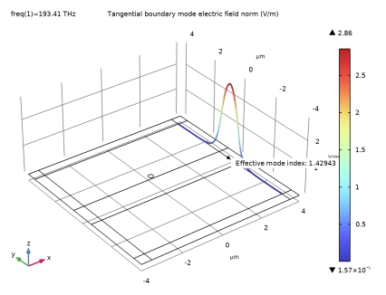
Electric Mode Field, Port 1 (ewfd)
Plot the first mode at port 1.
In the Model Builder window, click Electric Mode Field, Port 1 (ewfd).
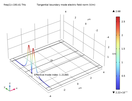
Electric Mode Field, Port 2 (ewfd)
Plot the first mode at port 2.
In the Model Builder window, click Electric Mode Field, Port 2 (ewfd).
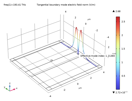
Electric Mode Field, Port 3 (ewfd)
Plot the second mode at port 1.
In the Model Builder window, click Electric Mode Field, Port 3 (ewfd).
Electric Mode Field, Port 4 (ewfd)
Plot the second mode at port 2.
In the Model Builder window, click Electric Mode Field, Port 4 (ewfd).
Electric Field (ewfd)
Plot the resistive losses in the gold scatterer.
Losses
1
In the Model Builder window, right-click Electric Field (ewfd) and choose Duplicate.
2
In the Settings window for 2D Plot Group, type Losses in the Label text field.
3
Click to expand the Selection section. Click  Clear Selection.
4
Surface 1
1
In the Model Builder window, expand the Losses node, then click Surface 1.
2
In the Settings window for Surface, locate the Expression section.
3
In the Expression text field, type ewfd.Qrh.
4
Locate the Coloring and Style section. From the Color table list, choose HeatCameraLight.
5
Click the  Zoom Extents button in the Graphics toolbar.
Reflectance, Transmittance, and Loss (ewfd)
As the total absorptance variable, ewfd.Atotal, only includes the loss due to absorption in the Gold domain, add a variable accounting for the loss due to power flowing into the top and bottom PML domains and for radiation not matching the port mode fields, ewfd.Lsca.
1
In the Model Builder window, under Results click Reflectance, Transmittance, and Absorptance (ewfd).
2
In the Settings window for Evaluation Group, type Reflectance, Transmittance, and Loss (ewfd) in the Label text field.
Reflectance, Transmittance, and Loss (ewfd)
1
In the Model Builder window, expand the Reflectance, Transmittance, and Loss (ewfd) node, then click Reflectance, Transmittance, and Absorptance (ewfd).
2
In the Settings window for Global Evaluation, type Reflectance, Transmittance, and Loss (ewfd) in the Label text field.
3
Click Add Expression in the upper-right corner of the Expressions section. From the menu, choose Component 1 (comp1) > Electromagnetic Waves, Frequency Domain > Heating and losses > ewfd.Lsca - Scattering loss - 1.
4
In the Reflectance, Transmittance, and Loss (ewfd) toolbar, click  Evaluate.
Loss Calculation
Also add a separate Global Evaluation node to separately calculate the absorptance, scattering, and total loss.
1
In the Results toolbar, click  Global Evaluation.
2
In the Settings window for Global Evaluation, type Loss Calculation in the Label text field.
3
Click Replace Expression in the upper-right corner of the Expressions section. From the menu, choose Component 1 (comp1) > Electromagnetic Waves, Frequency Domain > Heating and losses > ewfd.Atotal - Absorptance - 1.
4
Click Add Expression in the upper-right corner of the Expressions section. From the menu, choose Component 1 (comp1) > Electromagnetic Waves, Frequency Domain > Heating and losses > ewfd.Lsca - Scattering loss - 1.
5
Locate the Expressions section. In the table, enter the following settings:
6
Click  Evaluate.