PDF

Waveguide S-Bend
Introduction
In optical waveguides, light propagates along a predefined path. The light wave is also confined in the dimensions perpendicular to the propagation direction. This is contrary to plane waves that have infinite spatial extension.
The guiding mechanism is most often based on total internal reflection. That is, if a wave reaches an interface between two media, it will be completely reflected if the refractive index in the incident medium is larger than the refractive index on the transmission side and the angle of incidence is larger than a certain angle.
The material domain with the higher refractive index is normally called the core domain and the surrounding domains are called the cladding domains. The cross section of the core domains can be circular, as for optical fibers (see the Step-Index Fiber Bend model), or rectangular, which is more common for integrated optical waveguides. The Optical Ring Resonator Notch Filter 3D model is an example of a rectangular waveguide structure.
The length of optical waveguides is often much longer than the wavelength of the light that propagates through the guides. To accommodate that requirement, the Electromagnetic Waves, Beam Envelopes interface is available in the Wave Optics Module. With that physics interface, it is possible to simulate the propagation of waves over distances that are much longer than the wavelength, as the mesh does not have to resolve the wavelength. Instead, if you define the electric field as
(1),
and you can provide a good approximation for the rapidly varying phase function ϕ(r), the amplitude or enveloped function E0(r) will vary very slowly. Then, when you solve for E0(r), a very coarse mesh can be used.
However, a problem with the approach described above, is that it can be difficult to provide the required guess for the phase function ϕ(r), if the waveguide structure is more complex. In this model, it is shown how to define auxiliary partial differential equations to solve for a good approximation of the phase function ϕ(r).
In addition, since the simulation is performed in 2D and the waveguide length is not too long, a comparison is also made with results using the Electromagnetic Waves, Frequency Domain interface. Notice though, that the Electromagnetic Waves, Frequency Domain interface cannot be used for solving more realistic optical waveguide problems in 3D and for longer propagation lengths, as that physics interface requires that the mesh resolves the waves on a wavelength scale.
Model Definition
This model simulates a waveguide S-bend. To build the geometry, parts from the Wave Optics Module Parts library are used. This simplifies the process considerably, when creating complex waveguide structures.
An additional advantage gained when using the parts, is that selections can easily be defined for materials and boundary conditions, etc.
To provide the required phase input for the Electromagnetic Waves, Beam Envelopes interface, two auxiliary General Form interfaces are added to the model. The first General Form interface computes the propagation length, s, along the waveguide core, whereas the second General Form interface computes the propagation length in the cladding domain. Using two interfaces, and solving first separately for that in the core, guarantees that the resulting expression for the wave vector is tangential to the core-cladding interface. The boundary conditions in the two physics interfaces make sure the propagation length variable, s, is everywhere continuous. Furthermore, a constraint is added to make the propagation length constant at the output boundary, after the S-bend. This makes it easier to define a continuous phase expression for all domains, including the Perfectly Matched Layer (PML) domains.
As the waveguide is bent, the excited wave will be converted to higher order modes. To make sure that these modes are absorbed, the waveguide structure is terminated by PML domains.
In Study 1, the propagation length approximation is first solved for using Stationary study steps for the General Form interfaces. The approximate propagation length is then used for defining the phase expression in Variable nodes, found under the Definitions node in the Model Builder tree. As Numeric ports are used, Boundary Mode Analysis study steps are used for solving for the port mode fields. Finally, a Frequency Domain study step solves for the electric field envelope, using the previously computed phase approximation and port mode fields.
In Study 2, the electric field is solved for using the Electromagnetic Waves, Frequency Domain interface. Also here, Numeric ports, backed by PMLs, are used.
Results and Discussion
Figure 1 shows the electric field norm for the wave propagating along the waveguide S-bend, when using the Electromagnetic Waves, Beam Envelopes interface.
Figure 1: The electric field norm along the waveguide S-bend, when using the Electromagnetic Waves, Beam Envelopes interface.
Figure 2 show the phase approximation, computed by the General Form interfaces and used by the Electromagnetic Waves, Beam Envelopes interface. Notice that it is everywhere continuous and that the phase fronts in the core are orthogonal to the core-cladding boundaries.
Figure 2: Surface and contour plots of the phase along the waveguide structure. The arrows represent the wave vector, defined as the gradient of the phase, that is used by the Electromagnetic Waves, Beam Envelopes interface.
Figure 3 shows the z component of the electric field envelope. Thanks to the good provided phase approximation, the envelope function has a very slow variation along the waveguide. However, it is clear from the plot that higher order radiation is generated due to the waveguide bends.
Figure 3: The z component of the electric field envelope.
Figure 4 shows a comparison between the electric field norms, when computed by the Electromagnetic Waves, Beam Envelopes and Electromagnetic Waves, Frequency Domain interfaces, respectively. Notice that the field plots are almost the same for the two interfaces.
Figure 4: The electric field norms computed by the Electromagnetic Waves, Beam Envelopes (left) and the Electromagnetic Waves, Frequency Domain (right) interfaces, respectively.
Finally, Figure 5 shows a comparison similar to that in Figure 4, but here the plots show the expressions 20*log10(<tag>.normE) (<tag> is the physics interface tag – ewbe and ewfd, respectively). This comparison shows that the field values are very similar for the range from 30 dB to more than 85 dB.
Figure 5: Same kind of comparison as in Figure 4, but using dB scale.
Application Library path: Wave_Optics_Module/Waveguides/waveguide_s_bend
Modeling Instructions
From the File menu, choose New.
New
In the New window, click  Model Wizard.
Model Wizard
1
In the Model Wizard window, click  2D.
2
In the Select Physics tree, select Optics > Wave Optics > Electromagnetic Waves, Beam Envelopes (ewbe), Optics > Wave Optics > Electromagnetic Waves, Frequency Domain (ewfd), and Mathematics > PDE Interfaces > General Form PDE (g).
3
Click Add.
4
In the Select Physics tree, select Mathematics > PDE Interfaces > General Form PDE (g).
5
Click Add.
6
Click  Study.
7
In the Select Study tree, select Preset Studies for Some Physics Interfaces > Boundary Mode Analysis.
8
Global Definitions
Parameters 1
1
In the Model Builder window, under Global Definitions click Parameters 1.
2
In the Settings window for Parameters, locate the Parameters section.
3
Click  Load from File.
4
The parameters above define the operation wavelength, the geometry dimensions, and the material properties.
Part Libraries
Build the geometry using parts from the Wave Optics Module Parts library.
1
In the Home toolbar, click  Windows and choose Part Libraries.
2
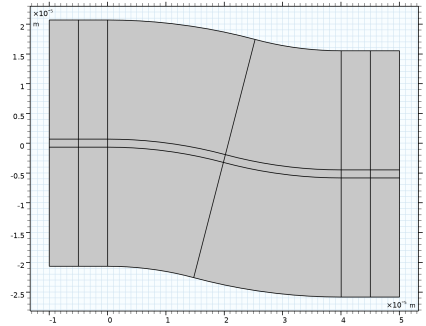
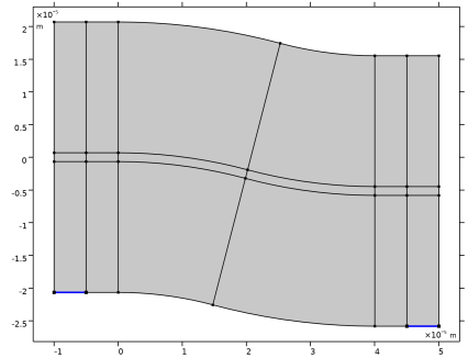
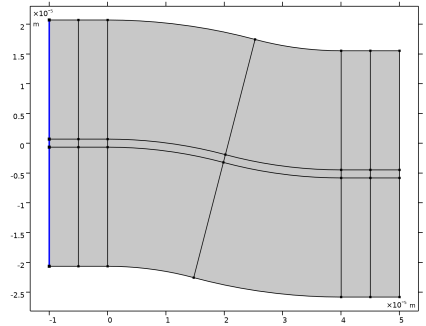
In the Part Libraries window, select Wave Optics Module > Slab Waveguides > slab_waveguide_s_bend in the tree.
3
Click  Add to Geometry.
Geometry 1
Slab Waveguide S-Bend 1 (pi1)
1
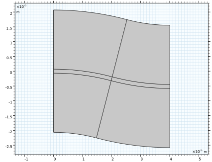
In the Model Builder window, under Component 1 (comp1) > Geometry 1 click Slab Waveguide S-Bend 1 (pi1).
2
In the Settings window for Part Instance, locate the Input Parameters section.
3
Notice that the core_offset parameter should not be changed.
4
Locate the Position and Orientation of Output section. In the Rotation angle text field, type -90.
5
Click  Build Selected.
6
Click to expand the Domain Selections section. Click New Cumulative Selection.
7
In the New Cumulative Selection dialog, type Core in the Name text field.
8
9
In the Settings window for Part Instance, locate the Domain Selections section.
10
Click New Cumulative Selection.
11
In the New Cumulative Selection dialog, type Cladding in the Name text field.
12
13
In the Settings window for Part Instance, locate the Domain Selections section.
14
Click New Cumulative Selection.
15
In the New Cumulative Selection dialog, type Non-PML in the Name text field.
16
17
In the Settings window for Part Instance, locate the Domain Selections section.
18
Part Libraries
1
In the Home toolbar, click  Windows and choose Part Libraries.
2
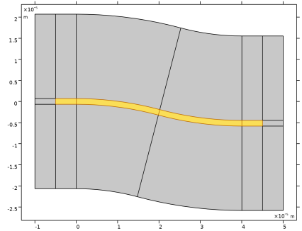
In the Part Libraries window, select Wave Optics Module > Slab Waveguides > slab_waveguide_straight in the tree.
3
Click  Add to Geometry.
Geometry 1
Slab Waveguide Straight 1 (pi2)
1
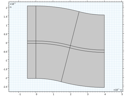
In the Model Builder window, under Component 1 (comp1) > Geometry 1 click Slab Waveguide Straight 1 (pi2).
2
In the Settings window for Part Instance, locate the Input Parameters section.
3
Again, do not change the value for the core_offset parameter.
4
Locate the Position and Orientation of Output section. In the Rotation angle text field, type 90.
5
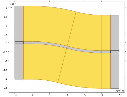
Locate the Domain Selections section. In the table, enter the following settings:
6
Click to expand the Boundary Selections section. Click to select row number 7 in the table.
7
Click New Cumulative Selection.
8
In the New Cumulative Selection dialog, type Port 1 in the Name text field.
9
10
In the Settings window for Part Instance, click  Build Selected.
Slab Waveguide Straight 2 (pi3)
1
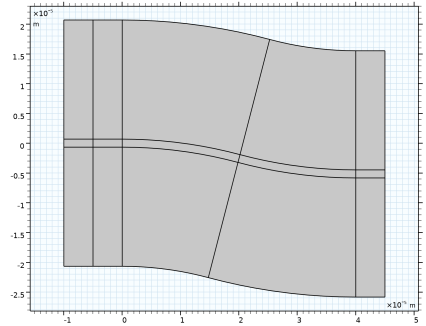
Right-click Component 1 (comp1) > Geometry 1 > Slab Waveguide Straight 1 (pi2) and choose Duplicate.
2
In the Settings window for Part Instance, locate the Position and Orientation of Output section.
3
In the x-displacement text field, type -d_straight_wg/2.
4
Locate the Domain Selections section. Click New Cumulative Selection.
5
In the New Cumulative Selection dialog, type Left PML in the Name text field.
6
7
In the Settings window for Part Instance, locate the Domain Selections section.
8
9
Locate the Boundary Selections section. In the table, enter the following settings:
10
Click  Build Selected.
Slab Waveguide Straight 3 (pi4)
1
Right-click Slab Waveguide Straight 1 (pi2) and choose Duplicate.
2
In the Settings window for Part Instance, locate the Position and Orientation of Output section.
3
In the x-displacement text field, type d_bent_wg.
4
In the y-displacement text field, type -offset.
5
In the Rotation angle text field, type -90.
6
Locate the Boundary Selections section. Click New Cumulative Selection.
7
In the New Cumulative Selection dialog, type Port 2 in the Name text field.
8
9
In the Settings window for Part Instance, locate the Boundary Selections section.
10
11
Click  Build Selected.
Slab Waveguide Straight 4 (pi5)
1
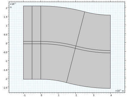
In the Model Builder window, under Component 1 (comp1) > Geometry 1 right-click Slab Waveguide Straight 2 (pi3) and choose Duplicate.
2
In the Settings window for Part Instance, locate the Position and Orientation of Output section.
3
In the x-displacement text field, type d_bent_wg+d_straight_wg/2.
4
In the y-displacement text field, type -offset.
5
In the Rotation angle text field, type -90.
6
Click  Build All Objects.
7
Locate the Domain Selections section. Click New Cumulative Selection.
8
In the New Cumulative Selection dialog, type Right PML in the Name text field.
9
10
In the Settings window for Part Instance, locate the Domain Selections section.
11
Now, add some selections to make it easier to add selections for materials and physics features.
PML
1
In the Geometry toolbar, click  Selections and choose Union Selection.
2
In the Settings window for Union Selection, type PML in the Label text field.
3
Locate the Input Entities section. Click  Add.
4
In the Add dialog, in the Selections to add list, choose Left PML and Right PML.
5
Definitions
Non-PML Core
1
In the Definitions toolbar, click  Intersection.
2
In the Settings window for Intersection, type Non-PML Core in the Label text field.
3
Locate the Input Entities section. Under Selections to intersect, click  Add.
4
In the Add dialog, in the Selections to intersect list, choose Core and Non-PML.
5
Non-PML Cladding
1
Right-click Non-PML Core and choose Duplicate.
2
In the Settings window for Intersection, type Non-PML Cladding in the Label text field.
3
Locate the Input Entities section. In the Selections to intersect list box, select Core.
4
Under Selections to intersect, click  Delete.
5
Under Selections to intersect, click  Add.
6
In the Add dialog, select Cladding in the Selections to intersect list.
7
Non-PML Core Boundaries
1
In the Definitions toolbar, click  Adjacent.
2
In the Settings window for Adjacent, type Non-PML Core Boundaries in the Label text field.
3
Locate the Input Entities section. Under Input selections, click  Add.
4
In the Add dialog, select Non-PML Core in the Input selections list.
5
Non-PML Cladding Boundaries
1
Right-click Non-PML Core Boundaries and choose Duplicate.
2
In the Settings window for Adjacent, type Non-PML Cladding Boundaries in the Label text field.
3
Locate the Input Entities section. In the Input selections list box, select Non-PML Core.
4
Under Input selections, click  Delete.
5
Under Input selections, click  Add.
6
In the Add dialog, select Non-PML Cladding in the Input selections list.
7
Non-PML Core-Cladding Boundaries
1
In the Definitions toolbar, click  Intersection.
2
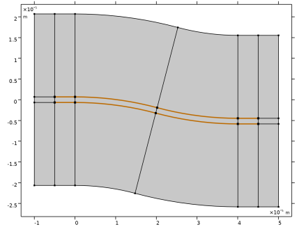
In the Settings window for Intersection, type Non-PML Core-Cladding Boundaries in the Label text field.
3
Locate the Geometric Entity Level section. From the Level list, choose Boundary.
4
Locate the Input Entities section. Under Selections to intersect, click  Add.
5
In the Add dialog, in the Selections to intersect list, choose Non-PML Core Boundaries and Non-PML Cladding Boundaries.
6
Materials
Cladding
1
In the Model Builder window, under Component 1 (comp1) right-click Materials and choose Blank Material.
2
In the Settings window for Material, type Cladding in the Label text field.
3
Locate the Material Contents section. In the table, enter the following settings:
Core
1
Right-click Materials and choose Blank Material.
2
In the Settings window for Material, type Core in the Label text field.
3
Locate the Geometric Entity Selection section. From the Selection list, choose Core.
4
Locate the Material Contents section. In the table, enter the following settings:
Electromagnetic Waves, Beam Envelopes (ewbe)
Port 1
1
In the Physics toolbar, click  Boundaries and choose Port.
2
In the Settings window for Port, locate the Boundary Selection section.
3
From the Selection list, choose Port 1.
4
Locate the Port Properties section. From the Type of port list, choose Numeric.
5
Select the Activate slit condition on interior port checkbox.
6
Click Toggle Power Flow Direction, to make the arrows in the Graphics window point toward the waveguide S-bend.
Port 2
1
In the Physics toolbar, click  Boundaries and choose Port.
2
In the Settings window for Port, locate the Boundary Selection section.
3
From the Selection list, choose Port 2.
4
Locate the Port Properties section. From the Type of port list, choose Numeric.
5
Select the Activate slit condition on interior port checkbox.
6
Click Toggle Power Flow Direction, to make the arrows in the Graphics window point away from the S-bend.
Port 1, Port 2
1
In the Model Builder window, under Component 1 (comp1) > Electromagnetic Waves, Beam Envelopes (ewbe), Ctrl-click to select Port 1 and Port 2.
2
Electromagnetic Waves, Frequency Domain (ewfd)
In the Model Builder window, under Component 1 (comp1) right-click Electromagnetic Waves, Frequency Domain (ewfd) and choose Paste Multiple Items.
General Form PDE (g)
1
In the Settings window for General Form PDE, locate the Domain Selection section.
2
From the Selection list, choose Non-PML Core.
3
Locate the Units section. Click  Select Dependent Variable Quantity.
4
In the Physical Quantity dialog, type Length in the text field.
5
In the tree, select General > Length (m).
6
7
In the Settings window for General Form PDE, locate the Units section.
8
In the Source term quantity table, enter the following settings:
General Form PDE 1
1
In the Model Builder window, under Component 1 (comp1) > General Form PDE (g) click General Form PDE 1.
2
In the Settings window for General Form PDE, locate the Source Term section.
3
In the f text field, type 0.
4
Locate the Damping or Mass Coefficient section. In the da text field, type 0.
Dirichlet Boundary Condition 1
1
In the Physics toolbar, click  Boundaries and choose Dirichlet Boundary Condition.
2
In the Settings window for Dirichlet Boundary Condition, locate the Boundary Selection section.
3
From the Selection list, choose Port 1.
4
Locate the Dirichlet Boundary Condition section. In the r text field, type -d_straight_wg/2.
Flux/Source 1
1
In the Physics toolbar, click  Boundaries and choose Flux/Source.
2
In the Settings window for Flux/Source, locate the Boundary Selection section.
3
From the Selection list, choose Port 2.
4
Locate the Boundary Flux/Source section. In the g text field, type 1, to make the x-derivative of u be 1[m]/1[m] = 1.
Now, add a global variable that will make the path length constant on the Port 2 boundary.
Global Equations 1 (ODE1)
1
In the Physics toolbar, click  Global and choose Global Equations.
2
In the Settings window for Global Equations, locate the Global Equations section.
3
4
Locate the Units section. Click  Select Dependent Variable Quantity.
5
In the Physical Quantity dialog, type Length in the text field.
6
In the tree, select General > Length (m).
7
Constraint 1
1
In the Physics toolbar, click  Boundaries and choose Constraint.
2
In the Settings window for Constraint, locate the Boundary Selection section.
3
From the Selection list, choose Port 2.
4
Locate the Constraint section. In the R text field, type u0-u. This is the constraint that will make the path length constant on the Port 2 boundary.
General Form PDE 2 (g2)
1
In the Model Builder window, under Component 1 (comp1) click General Form PDE 2 (g2).
2
In the Settings window for General Form PDE, locate the Domain Selection section.
3
From the Selection list, choose Non-PML Cladding.
4
Locate the Units section. Click  Select Dependent Variable Quantity.
5
In the Physical Quantity dialog, type Length in the text field.
6
In the tree, select General > Length (m).
7
8
In the Settings window for General Form PDE, locate the Units section.
9
In the Source term quantity table, enter the following settings:
General Form PDE 1
1
In the Model Builder window, under Component 1 (comp1) > General Form PDE 2 (g2) click General Form PDE 1.
2
In the Settings window for General Form PDE, locate the Source Term section.
3
In the f text field, type 0.
4
Locate the Damping or Mass Coefficient section. In the da text field, type 0.
General Form PDE (g)
Constraint 1, Dirichlet Boundary Condition 1, Flux/Source 1
1
In the Model Builder window, under Component 1 (comp1) > General Form PDE (g), Ctrl-click to select Dirichlet Boundary Condition 1, Flux/Source 1, and Constraint 1.
2
General Form PDE 2 (g2)
In the Model Builder window, under Component 1 (comp1) right-click General Form PDE 2 (g2) and choose Paste Multiple Items.
Constraint 1
1
In the Settings window for Constraint, locate the Constraint section.
2
In the R text field, type u0-u2.
Dirichlet Boundary Condition 2
1
In the Model Builder window, under Component 1 (comp1) > General Form PDE 2 (g2) right-click Dirichlet Boundary Condition 1 and choose Duplicate.
2
In the Settings window for Dirichlet Boundary Condition, locate the Boundary Selection section.
3
From the Selection list, choose Non-PML Core-Cladding Boundaries.
4
Locate the Dirichlet Boundary Condition section. In the r text field, type u.
Definitions
Perfectly Matched Layer 1 (pml1)
1
In the Definitions toolbar, click  Perfectly Matched Layer.
2
In the Settings window for Perfectly Matched Layer, locate the Domain Selection section.
3
From the Selection list, choose PML.
Perfectly Matched Layer 2 (pml2)
1
Right-click Perfectly Matched Layer 1 (pml1) and choose Duplicate.
2
In the Settings window for Perfectly Matched Layer, locate the Scaling section.
3
From the Physics list, choose Electromagnetic Waves, Frequency Domain (ewfd).
Core Path Length
1
In the Model Builder window, under Component 1 (comp1) right-click Definitions and choose Variables.
2
In the Settings window for Variables, type Core Path Length in the Label text field.
3
Locate the Geometric Entity Selection section. From the Geometric entity level list, choose Domain.
4
From the Selection list, choose Non-PML Core.
5
Locate the Variables section. In the table, enter the following settings:
Cladding Path Length
1
Right-click Core Path Length and choose Duplicate.
2
In the Settings window for Variables, type Cladding Path Length in the Label text field.
3
Locate the Geometric Entity Selection section. From the Selection list, choose Non-PML Cladding.
4
Locate the Variables section. In the table, enter the following settings:
Left PML
1
In the Model Builder window, right-click Definitions and choose Variables.
2
In the Settings window for Variables, type Left PML in the Label text field.
3
Locate the Geometric Entity Selection section. From the Geometric entity level list, choose Domain.
4
From the Selection list, choose Left PML.
5
Locate the Variables section. In the table, enter the following settings:
The variables above will be used later when finishing the definitions for the Electromagnetic Waves, Beam Envelopes interface.
Non-PML
1
Right-click Left PML and choose Duplicate.
2
In the Settings window for Variables, type Non-PML in the Label text field.
3
Locate the Geometric Entity Selection section. From the Selection list, choose Non-PML.
4
Locate the Variables section. In the table, enter the following settings:
Right PML
1
Right-click Non-PML and choose Duplicate.
2
In the Settings window for Variables, type Right PML in the Label text field.
3
Locate the Geometric Entity Selection section. From the Selection list, choose Right PML.
4
Locate the Variables section. In the table, enter the following settings:
Electromagnetic Waves, Beam Envelopes (ewbe)
Now, finalize the settings for this physics interface, using the variables defined in the previous steps.
1
In the Model Builder window, under Component 1 (comp1) click Electromagnetic Waves, Beam Envelopes (ewbe).
2
In the Settings window for Electromagnetic Waves, Beam Envelopes, locate the Components section.
3
From the Electric field components solved for list, choose Out-of-plane vector.
4
Locate the Wave Vectors section. From the Number of directions list, choose Unidirectional.
5
From the Type of phase specification list, choose User defined.
6
In the ϕ1 text field, type phi.
7
Click to expand the User-Defined Wave Vector Specification section. Specify the k1 vector as
It is necessary to use a User defined Type of phase specification with the special variables previously defined, because the default expression (d(phi,x), d(phi,y)) for the wave vector would give wrong attenuation in the PML domains.
Mapped Mesh
1
In the Model Builder window, under Component 1 (comp1) click Mesh 1.
2
In the Settings window for Mesh, type Mapped Mesh in the Label text field.
PML Distribution
1
Right-click Component 1 (comp1) > Mapped Mesh and choose Distribution.
2
In the Settings window for Distribution, type PML Distribution in the Label text field.
3
4
Locate the Distribution section. In the Number of elements text field, type 10.
Size Along Waveguide
1
In the Model Builder window, click Size.
2
In the Settings window for Size, type Size Along Waveguide in the Label text field.
3
Locate the Element Size section. Click the Custom button.
4
Locate the Element Size Parameters section. In the Maximum element size text field, type 2*lda0.
Core Size
1
In the Model Builder window, right-click Mapped Mesh and choose Size.
2
In the Settings window for Size, type Core Size in the Label text field.
3
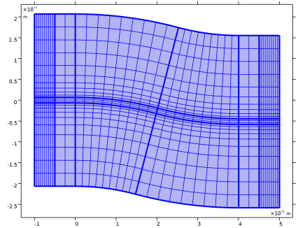
Locate the Geometric Entity Selection section. From the Geometric entity level list, choose Boundary.
4
5
Locate the Element Size section. Click the Custom button.
6
Locate the Element Size Parameters section.
7
Select the Maximum element size checkbox. In the associated text field, type w_core/3.
Left Edge
1
In the Mesh toolbar, click  More Generators and choose Edge.
2
In the Settings window for Edge, type Left Edge in the Label text field.
3
Mapped 1
1
In the Mesh toolbar, click  Mapped.
2
In the Settings window for Mapped, click to expand the Reduce Element Skewness section.
3
Select the Adjust edge mesh checkbox.
4
Click  Build All.
Study 1
Step 1: Boundary Mode Analysis
1
In the Model Builder window, under Study 1 click Step 1: Boundary Mode Analysis.
2
In the Settings window for Boundary Mode Analysis, locate the Study Settings section.
3
In the Mode analysis frequency text field, type f0.
4
Select the Search for modes around shift checkbox. In the associated text field, type n_core.
5
Locate the Physics and Variables Selection section. In the Solve for column of the table, under Component 1 (comp1), clear the checkboxes for Electromagnetic Waves, Frequency Domain (ewfd), General Form PDE (g), and General Form PDE 2 (g2).
Step 3: Boundary Mode Analysis 1
1
Right-click Study 1 > Step 1: Boundary Mode Analysis and choose Duplicate.
2
Right-click Step 3: Boundary Mode Analysis 1 and choose Move Up.
3
In the Settings window for Boundary Mode Analysis, locate the Study Settings section.
4
In the Port name text field, type 2.
Step 3: Frequency Domain
1
In the Model Builder window, click Step 3: Frequency Domain.
2
In the Settings window for Frequency Domain, locate the Study Settings section.
3
In the Frequencies text field, type f0.
4
Locate the Physics and Variables Selection section. Select the Modify model configuration for study step checkbox.
5
In the tree, select Component 1 (comp1) > Definitions > Artificial Domains > Perfectly Matched Layer 2 (pml2).
6
Click  Disable.
7
In the tree, select Component 1 (comp1) > Electromagnetic Waves, Frequency Domain (ewfd).
8
Click  Disable in Solvers.
9
In the tree, select Component 1 (comp1) > General Form PDE (g).
10
Click  Disable in Solvers.
11
In the tree, select Component 1 (comp1) > General Form PDE 2 (g2).
12
Click  Disable in Solvers.
Step 4: Stationary
1
In the Study toolbar, click  Stationary.
2
Drag and drop above Step 2: Boundary Mode Analysis.
3
In the Settings window for Stationary, locate the Physics and Variables Selection section.
4
In the Solve for column of the table, under Component 1 (comp1), clear the checkbox for General Form PDE 2 (g2).
Step 5: Stationary 1
1
Right-click Study 1 > Step 1: Stationary and choose Duplicate.
2
Drag and drop Step 5: Stationary 1 below Step 1: Stationary.
3
In the Settings window for Stationary, locate the Physics and Variables Selection section.
4
In the Solve for column of the table, under Component 1 (comp1), clear the checkbox for General Form PDE (g).
5
In the Solve for column of the table, under Component 1 (comp1), select the checkbox for General Form PDE 2 (g2).
6
In the Study toolbar, click  Compute.
Results
Height Expression 1
1
In the Model Builder window, expand the Results > Electric Field (ewbe) node.
2
Right-click Electric Field and choose Height Expression.
3
In the Settings window for Height Expression, locate the Axis section.
4
Select the Scale factor checkbox. In the associated text field, type 5e-10.
Electric Field
1
In the Model Builder window, click Electric Field.
2
In the Settings window for Surface, locate the Coloring and Style section.
3
From the Color table list, choose HeatCameraLight.
4
In the Electric Field (ewbe) toolbar, click  Plot.
5
Click the Zoom Box button on the Graphics toolbar and then use the mouse to zoom in.
This plot shows how the wave propagates along the S-bend.
Phase
1
In the Model Builder window, under Results click General Form PDE.
2
In the Settings window for 2D Plot Group, type Phase in the Label text field.
Surface 1
1
In the Model Builder window, expand the Phase node, then click Surface 1.
2
In the Settings window for Surface, locate the Expression section.
3
In the Expression text field, type phi.
Contour 1
1
In the Model Builder window, right-click Phase and choose Contour.
2
In the Settings window for Contour, locate the Expression section.
3
In the Expression text field, type phi.
4
Locate the Coloring and Style section. From the Coloring list, choose Uniform.
5
From the Color list, choose White.
6
Clear the Color legend checkbox.
Arrow Surface 1
1
Right-click Phase and choose Arrow Surface.
2
In the Settings window for Arrow Surface, locate the Expression section.
3
In the X-component text field, type k1x.
4
In the Y-component text field, type k1y.
5
In the Phase toolbar, click  Plot.
6
Click the  Zoom Extents button in the Graphics toolbar.
Amplitude, First Wave
1
In the Model Builder window, under Results click General Form PDE 2.
2
In the Settings window for 2D Plot Group, type Amplitude, First Wave in the Label text field.
3
Click to expand the Selection section. From the Geometric entity level list, choose Domain.
4
From the Selection list, choose Non-PML.
5
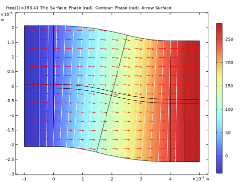
Select the Apply to dataset edges checkbox.
Surface 1
1
In the Model Builder window, expand the Amplitude, First Wave node, then click Surface 1.
2
In the Settings window for Surface, locate the Expression section.
3
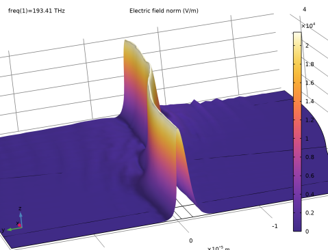
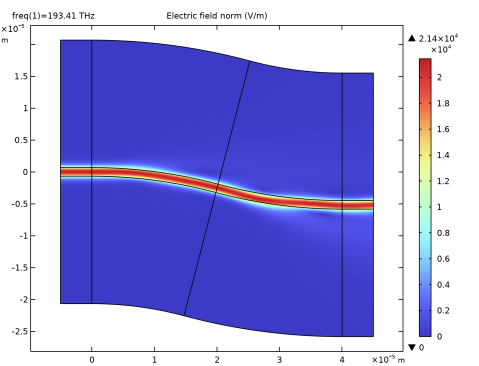
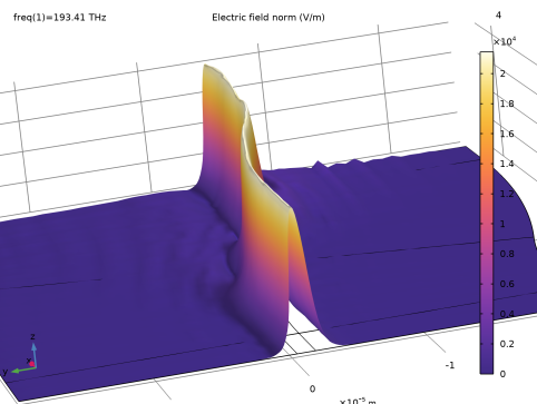
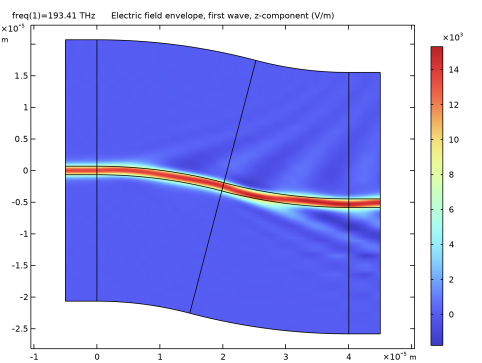
In the Expression text field, type E1z. This is the dependent variable solved for, the z component of the electric field envelope.
4
In the Amplitude, First Wave toolbar, click  Plot.
Notice that the amplitude is almost constant along the propagation path. However, it is also clear that part of the wave power is converted to higher order modes.
Reflectance, Transmittance, and Absorptance (ewbe)
The reflectance, transmittance, and loss values can be computed using the evaluation group.
1
In the Model Builder window, expand the Results > Reflectance, Transmittance, and Absorptance (ewbe) node, then click Reflectance, Transmittance, and Absorptance (ewbe).
2
In the Settings window for Global Evaluation, locate the Expressions section.
3
This variable calculates the loss for the radiation that does not match the port mode fields.
4
In the Reflectance, Transmittance, and Absorptance (ewbe) toolbar, click  Evaluate.
Electromagnetic Waves, Frequency Domain (ewfd)
1
In the Model Builder window, under Component 1 (comp1) click Electromagnetic Waves, Frequency Domain (ewfd).
2
In the Settings window for Electromagnetic Waves, Frequency Domain, locate the Components section.
3
From the Electric field components solved for list, choose Out-of-plane vector.
Triangular Mesh
1
In the Mesh toolbar, click Add Mesh and choose Add Mesh.
2
In the Settings window for Mesh, type Triangular Mesh in the Label text field.
3
Locate the Physics-Controlled Mesh section. In the table, clear the Use checkboxes for Electromagnetic Waves, Beam Envelopes (ewbe), General Form PDE (g), and General Form PDE 2 (g2).
4
Click  Build All.
Notice that this mesh is much denser than the mesh used by the Electromagnetic Waves, Beam Envelopes interface.
Add Study
1
In the Home toolbar, click  Add Study to open the Add Study window.
2
Go to the Add Study window.
3
Find the Studies subsection. In the Select Study tree, select Empty Study.
4
Click the Add Study button in the window toolbar.
Study 1
Step 3: Boundary Mode Analysis, Step 4: Boundary Mode Analysis 1, Step 5: Frequency Domain
1
In the Model Builder window, under Study 1, Ctrl-click to select Step 3: Boundary Mode Analysis, Step 4: Boundary Mode Analysis 1, and Step 5: Frequency Domain.
2
Study 2
In the Model Builder window, right-click Study 2 and choose Paste Multiple Items.
Step 1: Boundary Mode Analysis
1
In the Settings window for Boundary Mode Analysis, locate the Physics and Variables Selection section.
2
In the Solve for column of the table, under Component 1 (comp1), clear the checkbox for Electromagnetic Waves, Beam Envelopes (ewbe).
3
In the Solve for column of the table, under Component 1 (comp1), select the checkbox for Electromagnetic Waves, Frequency Domain (ewfd).
4
Click to expand the Mesh Selection section. In the table, enter the following settings:
Step 2: Boundary Mode Analysis 1
1
In the Model Builder window, click Step 2: Boundary Mode Analysis 1.
2
In the Settings window for Boundary Mode Analysis, locate the Physics and Variables Selection section.
3
In the Solve for column of the table, under Component 1 (comp1), clear the checkbox for Electromagnetic Waves, Beam Envelopes (ewbe).
4
In the Solve for column of the table, under Component 1 (comp1), select the checkbox for Electromagnetic Waves, Frequency Domain (ewfd).
5
Click to expand the Mesh Selection section. In the table, enter the following settings:
Step 3: Frequency Domain
1
In the Model Builder window, click Step 3: Frequency Domain.
2
In the Settings window for Frequency Domain, locate the Physics and Variables Selection section.
3
In the tree, select Component 1 (comp1) > Definitions > Artificial Domains > Perfectly Matched Layer 1 (pml1).
4
Click  Disable.
5
In the tree, select Component 1 (comp1) > Definitions > Artificial Domains > Perfectly Matched Layer 2 (pml2).
6
Click  Enable.
7
In the tree, select Component 1 (comp1) > Electromagnetic Waves, Beam Envelopes (ewbe).
8
Click  Disable in Solvers.
9
In the tree, select Component 1 (comp1) > Electromagnetic Waves, Frequency Domain (ewfd).
10
Click  Solve For.
11
Click to expand the Mesh Selection section. In the table, enter the following settings:
12
In the Study toolbar, click  Add Study to close the Add Study window.
13
In the Study toolbar, click  Compute.
Results
Electric Field (ewfd)
1
In the Electric Field (ewfd) toolbar, click  Plot.
2
Click the  Zoom Extents button in the Graphics toolbar.
3
In the Model Builder window, under Results click Electric Field (ewfd).
This plot is very similar to the corresponding plot for the Electromagnetic Waves, Beam Envelopes interface. Next, we will add two plots comparing the electric fields computed by the two different electromagnetic waves physics interfaces.
Field Comparison, Linear Scale
1
Right-click Electric Field (ewfd) and choose Duplicate.
2
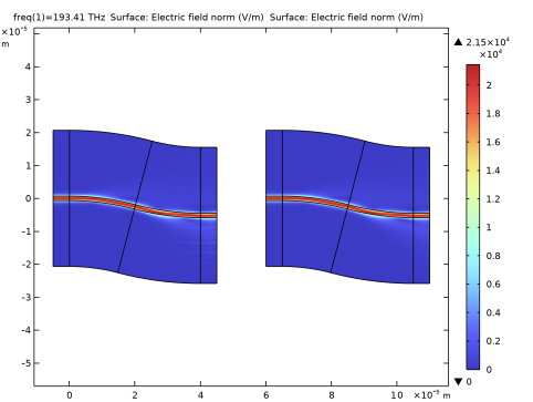
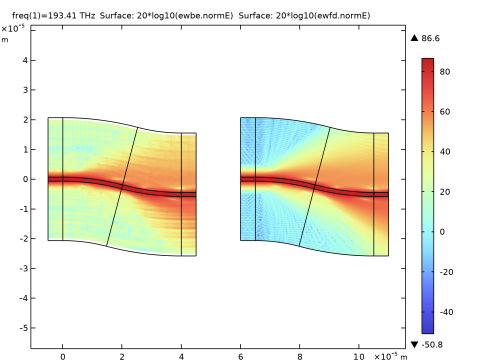
In the Settings window for 2D Plot Group, type Field Comparison, Linear Scale in the Label text field.
3
Locate the Data section. From the Dataset list, choose Study 1/Solution 1 (sol1).
4
Click to expand the Plot Array section. From the Array type list, choose Linear.
Surface 2
1
In the Model Builder window, expand the Field Comparison, Linear Scale node.
2
Right-click Results > Field Comparison, Linear Scale > Surface 1 and choose Duplicate.
3
In the Settings window for Surface, locate the Data section.
4
From the Dataset list, choose Study 2/Solution 6 (sol6).
5
Click to expand the Inherit Style section. From the Plot list, choose Surface 1.
Surface 1
1
In the Model Builder window, click Surface 1.
2
In the Settings window for Surface, locate the Expression section.
3
In the Expression text field, type ewbe.normE.
4
Click the  Zoom Extents button in the Graphics toolbar.
5
In the Field Comparison, Linear Scale toolbar, click  Plot.
This plot confirms that the result from the two different physics interfaces produce almost the same results.
Field Comparison, Linear Scale
Now, create a plot comparing the electric fields, using a logarithmic scale.
Field Comparison, Log Scale
1
In the Model Builder window, right-click Field Comparison, Linear Scale and choose Duplicate.
2
In the Model Builder window, click Field Comparison, Linear Scale 1.
3
In the Settings window for 2D Plot Group, type Field Comparison, Log Scale in the Label text field.
Surface 1
1
In the Model Builder window, click Surface 1.
2
In the Settings window for Surface, locate the Expression section.
3
In the Expression text field, type 20*log10(ewbe.normE).
Surface 2
1
In the Model Builder window, click Surface 2.
2
In the Settings window for Surface, locate the Expression section.
3
In the Expression text field, type 20*log10(ewfd.normE).
4
In the Field Comparison, Log Scale toolbar, click  Plot.
Also on a logarithmic scale, the results are very similar, for value above 40 dB.
Reflectance, Transmittance, and Absorptance (ewfd)
Finally, inspect the reflectance, transmittance, and loss values using the evaluation group.
1
In the Model Builder window, expand the Results > Reflectance, Transmittance, and Absorptance (ewfd) node, then click Reflectance, Transmittance, and Absorptance (ewfd).
2
In the Settings window for Global Evaluation, locate the Expressions section.
3
Again, as there is no material absorption in this model, it is more relevant to evaluate the amount of radiation that does not match the port mode fields.
4
In the Reflectance, Transmittance, and Absorptance (ewfd) toolbar, click  Evaluate.