PDF

Dispersion of Surface Plasmon Polariton in Thin Metal Embedded in Dielectric
Introduction
Surface plasmon polaritons (SPPs) are a special class of surface waves that propagate along the interface between materials with negative and positive dielectric constants, and decay in the direction normal to the interface. Most of the metals at optical frequencies possess a negative dielectric constant, and are widely used materials to excite such surface waves. An SPP propagates along the metal–dielectric interface until it completely loses its energy due to the metal absorption. The thickness of the metal layer plays an important role in this context as it controls the absorption of the structure.
In the case of a metal layer with a certain thickness, embedded in a dielectric, SPPs propagating on the top and bottom interfaces couple to each other and create a supermode. Such a structure behaves similarly to an optical slab waveguide with dispersion depending on the metal thickness. SPPs supported by thin metal layers could be useful in practical applications such as short-distance signal transmission and routing as well as to design power splitters and optical couplers.
Model Definition
The schematic of the model is shown in Figure 1. A thin metal layer is covered by layers of dielectrics with certain thickness and is surrounded by air.
The expressions of the electric and magnetic fields of the TM surface waves or SPPs and the propagation constant are available in Ref. 1.
As the SPPs propagate along the surface, they lose energy due to the metal absorption. The dispersion of the structure as well as the complex SPP wavenumber kspp = kr + iki depends on the thickness of metal. Assume that the SPP wave propagates along the x direction. The electric field component of such a wave is represented by
Therefore, at a distance x, the SPP intensity has decayed by a factor of . The propagation length, L of the SPP is defined as the distance at which the wave intensity decays by a factor 1/e, and is defined as
Figure 1: Schematic of the configuration. A thin metal layer is embedded in layers of dielectric with certain thickness. The setup is surrounded by air domains.
This model simulates SPPs propagating in a thin layer of aluminum embedded in dielectric layers, using material properties for aluminum from the built-in Optical Material Library. Numeric ports are used on the left and right boundaries of the model. The left port, with excitation turned on, launches the SPP, while the right port, with excitation turned off, absorbs the SPP without reflection. To get the mode field for both ports, two Boundary Mode Analysis study steps are added. Finally, another Boundary Mode Analysis study step with Auxiliary sweep of the wavelength is used to calculate the dispersion and the propagation length of SPP.
Results and Discussion
Figure 2 shows the electric field y-component of the SPP as it propagates from left to right. The intensity of the wave decays as it propagates due to metal absorption.
Figure 2: The y-component of the electric field for a wavelength of 290 nm (4.28 eV). The wave gets weaker, due to absorption, as it propagates from left to right.
Figure 3 shows the propagation constant of the SPP versus the photon energy and compares with the propagation constant of light in free space. As the photon energy reduces and moves away from the plasmon resonance frequency of aluminium, the SPP propagation constant converges with the propagation constant of free space light.
Figure 4 shows the propagation length versus the photon energy. The SPPs decay very fast when the photon energy is very high. This is due to the fact of strong metal absorption at high photon energy, and the loss gradually decreases as the photo energy reduces.
For more SPP simulation examples, see Ref. 1.
Figure 3: Photon energy versus the propagation constant.
Figure 4: Photon energy versus the propagation length.
Reference
1. X. Chen, “Modeling Surface Plasmon Polaritons in COMSOL®,” COMSOL Blog, 12 Oct. 2022; www.comsol.com/blogs/modeling-surface-plasmon-polaritons-in-comsol/.
Application Library path: Wave_Optics_Module/Waveguides/thin_metal_surface_plasmon_polariton
Modeling Instructions
From the File menu, choose New.
New
In the New window, click  Model Wizard.
Model Wizard
1
In the Model Wizard window, click  2D.
2
In the Select Physics tree, select Optics > Wave Optics > Electromagnetic Waves, Frequency Domain (ewfd).
3
Click Add.
4
Click  Study.
5
In the Select Study tree, select General Studies > Frequency Domain.
6
Geometry 1
1
In the Model Builder window, under Component 1 (comp1) click Geometry 1.
2
In the Settings window for Geometry, locate the Units section.
3
From the Length unit list, choose nm.
Global Definitions
Parameters 1
1
In the Model Builder window, under Global Definitions click Parameters 1.
2
In the Settings window for Parameters, locate the Parameters section.
3
Geometry 1
The geometry consists of a thin metal layer embedded in a dielectric. The structure is surrounded by air domain.
Rectangle 1 (r1)
1
In the Geometry toolbar, click  Rectangle.
2
In the Settings window for Rectangle, locate the Size and Shape section.
3
In the Width text field, type L.
4
In the Height text field, type H.
5
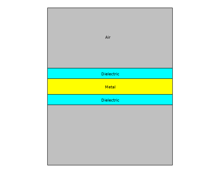
Click to expand the Layers section. In the table, enter the following settings:
6
Select the Layers on top checkbox.
7
Click  Build Selected.
In the Graphics window, click Zoom In twice to clearly visualize the metal and dielectric domains.
Rectangle 2 (r2)
Build another rectangle with similar width, and height equal to half of the total geometry. This will be useful to copy mesh from the top half of the geometry to the bottom half.
1
In the Geometry toolbar, click  Rectangle.
2
In the Settings window for Rectangle, locate the Size and Shape section.
3
In the Width text field, type L.
4
In the Height text field, type H/2.
5
Click  Build All Objects.
In the Graphics window, click Zoom In twice to clearly visualize the metal and dielectric domains.
Materials
Pick Aluminium as the metal from the Optical material library.
Add Material
1
In the Materials toolbar, click  Add Material to open the Add Material window.
2
Go to the Add Material window.
3
In the tree, select Built-in > Air.
4
Right-click and choose Add to Component 1 (comp1).
5
In the tree, select Optical > Inorganic Materials > Al - Aluminium and aluminates > Models and simulations > Al (Aluminium) (Rakic et al. 1998: Lorentz-Drude model; n,k 0.0620-248 um).
6
Right-click and choose Add to Component 1 (comp1).
7
In the Materials toolbar, click  Add Material to close the Add Material window.
Materials
Al (Aluminium) (Rakic et al. 1998: Lorentz-Drude model; n,k 0.0620-248 um) (mat2)
1
In the Graphics window, click Zoom In twice to clearly visualize the metal layer.
Dielectric
1
In the Model Builder window, right-click Materials and choose Blank Material.
2
In the Settings window for Material, type Dielectric in the Label text field.
3
In the Graphics window, click Zoom In twice to clearly visualize the dielectric domains.
4
Locate the Material Contents section. In the table, enter the following settings:
Electromagnetic Waves, Frequency Domain (ewfd)
Port 1
1
In the Physics toolbar, click  Boundaries and choose Port.
2
3
In the Settings window for Port, locate the Port Properties section.
4
From the Type of port list, choose Numeric.
Port 2
1
Right-click Port 1 and choose Duplicate.
2
In the Settings window for Port, locate the Boundary Selection section.
3
Click  Clear Selection.
4
5
Locate the Port Properties section. From the Wave excitation at this port list, choose Off.
Mesh 1
Distribution 1
1
In the Model Builder window, under Component 1 (comp1) right-click Mesh 1 and choose Distribution.
2
3
In the Settings window for Distribution, locate the Distribution section.
4
From the Distribution type list, choose Predefined.
5
In the Number of elements text field, type 20.
6
In the Element ratio text field, type 100.
7
From the Growth rate list, choose Exponential.
Size
1
In the Model Builder window, click Size.
2
In the Settings window for Size, click to expand the Element Size Parameters section.
3
In the Minimum element size text field, type 0.6.
Distribution 2
1
In the Model Builder window, under Component 1 (comp1) > Mesh 1 right-click Distribution 1 and choose Duplicate.
2
In the Settings window for Distribution, locate the Boundary Selection section.
3
Click  Clear Selection.
4
5
Locate the Distribution section. From the Distribution type list, choose Fixed number of elements.
6
In the Number of elements text field, type round(L/4[nm]).
Set each element size to 4 nm to properly resolve the surface plasmon polariton.
Distribution 3
1
Right-click Distribution 2 and choose Duplicate.
2
In the Settings window for Distribution, locate the Boundary Selection section.
3
Click  Clear Selection.
4
In the Graphics window, click Zoom to Selection to clearly visualize the boundary layer.
5
Locate the Distribution section. In the Number of elements text field, type 10.
Distribution 4
1
Right-click Distribution 3 and choose Duplicate.
2
In the Settings window for Distribution, locate the Boundary Selection section.
3
Click  Clear Selection.
4
In the Graphics window, click Zoom to Selection to clearly visualize the boundary layer.
5
Locate the Distribution section. In the Number of elements text field, type 25.
Mapped 1
1
In the Mesh toolbar, click  Mapped.
2
In the Settings window for Mapped, locate the Domain Selection section.
3
From the Geometric entity level list, choose Domain.
4
In the Graphics window, click Zoom to Selection to properly visualize the top half of the geometry.
Copy Domain 1
1
In the Model Builder window, right-click Mesh 1 and choose Copying Operations > Copy Domain.
2
3
In the Settings window for Copy Domain, locate the Destination Domains section.
4
Click to select the  Activate Selection toggle button.
5
6
Click  Build All.
Study 1
This study is used to simulate the field profile of surface plasmon polariton propagating in thin metal layer.
Step 1: Frequency Domain
1
In the Model Builder window, under Study 1 click Step 1: Frequency Domain.
2
In the Settings window for Frequency Domain, locate the Study Settings section.
3
In the Frequencies text field, type f0.
Step 2: Boundary Mode Analysis
1
In the Study toolbar, click  More Study Steps and choose Other > Boundary Mode Analysis.
2
In the Settings window for Boundary Mode Analysis, locate the Study Settings section.
3
In the Mode analysis frequency text field, type f0.
4
In the Search for modes around shift text field, type 1.4.
5
From the Search method around shift list, choose Larger real part.
Step 3: Boundary Mode Analysis 1
1
Right-click Step 2: Boundary Mode Analysis and choose Duplicate.
2
In the Settings window for Boundary Mode Analysis, locate the Study Settings section.
3
In the Port name text field, type 2.
Step 1: Frequency Domain
1
In the Model Builder window, click Step 1: Frequency Domain.
2
Drag and drop below Step 2: Boundary Mode Analysis 1.
3
In the Study toolbar, click  Compute.
Results
Surface 1
1
In the Model Builder window, expand the Electric Field (ewfd) node, then click Surface 1.
2
In the Settings window for Surface, locate the Expression section.
3
In the Expression text field, type ewfd.Ey.
4
Locate the Coloring and Style section. From the Color table list, choose Wave.
5
From the Scale list, choose Linear symmetric.
Electric Mode Field, Port 1 (ewfd)
In the Model Builder window, under Results click Electric Mode Field, Port 1 (ewfd).
Electric Mode Field, Port 2 (ewfd)
In the Model Builder window, click Electric Mode Field, Port 2 (ewfd).
Add Study
1
In the Home toolbar, click  Add Study to open the Add Study window.
2
Go to the Add Study window.
3
Find the Studies subsection. In the Select Study tree, select Empty Study.
4
Study 2
Add another study to calculate the dispersion of thin metal embedded in dielectric versus frequency.
1
In the Model Builder window, click Study 2.
2
In the Settings window for Study, locate the Study Settings section.
3
Clear the Generate default plots checkbox.
Step 1: Boundary Mode Analysis
1
In the Study toolbar, click  More Study Steps and choose Other > Boundary Mode Analysis.
2
In the Settings window for Boundary Mode Analysis, locate the Study Settings section.
3
In the Mode analysis frequency text field, type f0.
4
Select the Desired number of modes checkbox. In the associated text field, type 2.
5
From the Search method around shift list, choose Larger real part.
6
Click to expand the Study Extensions section. Select the Auxiliary sweep checkbox.
7
8
9
In the Home toolbar, click  Add Study to close the Add Study window.
10
In the Study toolbar, click  Compute.
Results
Propagation Constant
1
In the Results toolbar, click  1D Plot Group.
2
In the Settings window for 1D Plot Group, type Propagation Constant in the Label text field.
3
Locate the Data section. From the Dataset list, choose Study 2/Solution 4 (sol4).
4
Click to expand the Title section. From the Title type list, choose None.
5
Locate the Plot Settings section.
6
Select the x-axis label checkbox. In the associated text field, type Propagation constant (1/m).
7
Select the y-axis label checkbox. In the associated text field, type Photon energy (eV).
First, plot the propagation constant of surface plasmon polariton in thin metal layer embedded in a dielectric.
Global 1
1
Right-click Propagation Constant and choose Global.
2
In the Settings window for Global, locate the y-Axis Data section.
3
4
Locate the x-Axis Data section. From the Axis source data list, choose All solutions.
5
From the Parameter list, choose Expression.
6
In the Expression text field, type abs(ewfd.beta_1).
7
Click to expand the Coloring and Style section. Find the Line style subsection. From the Line list, choose None.
8
Find the Line markers subsection. From the Marker list, choose Circle.
9
Click to expand the Legends section. From the Legends list, choose Manual.
10
Color Expression 1
1
Right-click Global 1 and choose Color Expression.
2
In the Settings window for Color Expression, locate the Expression section.
3
In the Expression text field, type -real(ewfd.beta_1)/imag(ewfd.beta_1).
4
Locate the Coloring and Style section. From the Color table list, choose Viridis.
5
From the Scale list, choose Logarithmic.
Global 2
1
In the Model Builder window, right-click Propagation Constant and choose Global.
Now, plot the propagation constant of light in free space.
2
In the Settings window for Global, locate the y-Axis Data section.
3
4
Locate the x-Axis Data section. From the Axis source data list, choose All solutions.
5
From the Parameter list, choose Expression.
6
In the Expression text field, type ewfd.k0.
7
Locate the Coloring and Style section. Find the Line style subsection. From the Line list, choose Dashed.
8
From the Color list, choose Black.
9
Locate the Legends section. From the Legends list, choose Manual.
10
11
In the Propagation Constant toolbar, click  Plot.
Propagation Length
1
Right-click Propagation Constant and choose Duplicate.
Plot the propagation length of SPP.
2
In the Settings window for 1D Plot Group, type Propagation Length in the Label text field.
3
Locate the Plot Settings section. In the x-axis label text field, type Propagation length (nm).
4
Locate the Legend section. Clear the Show legends checkbox.
Global 1
1
In the Model Builder window, expand the Propagation Length node, then click Global 1.
2
In the Settings window for Global, locate the x-Axis Data section.
3
In the Expression text field, type 1/(2*real(ewfd.beta_1)).
Global 2
In the Model Builder window, right-click Global 2 and choose Delete.
Global 1