PDF

Scatterer on Substrate
Introduction
A plane TE-polarized electromagnetic wave is incident on a gold nanoparticle on a dielectric substrate. The absorption and scattering cross sections of the particle, and the far-field radiation pattern are computed for a few different polar and azimuthal angles of incidence.
Model Definition
Figure 1 shows the geometry, with the substrate considered to occupy the entire z < 0 half-space. A plane electromagnetic wave, with a 500 nm wavelength, is incident at a polar angle θ and an azimuthal angle ϕ. The wave is plane-polarized with the electric field vector tangential to the surface of the substrate.
Figure 1: The modeled geometry. The gray domain represents the dielectric substrate. The electric field vector of the incident wave points in the ϕ direction, orthogonal to the plane of incidence.
The model uses na = 1 for air and nb = 1.5 for the dielectric substrate. The scattering nanoparticle is made of gold. The refractive index is taken from the Optical Material Library.
The model computes the scattering, absorption, and extinction cross sections of the particle on the substrate. The scattering cross section is defined as
Here, n is the normal vector pointing outward from the scatterer, Ssc is the scattered intensity (Poynting) vector, and I0 is the incident intensity. The integral is taken over the closed surface of the scatterer. The absorption cross section equals
where Q is the power loss density in the particle and the integral is taken over its volume. The extinction cross section is simply the sum of the two others:
The model also calculates the far-field variables.
Results and Discussion
As explained in Notes About the COMSOL Implementation, the model first computes a background field from the plane wave incident on the substrate, and then uses that to arrive at the total field with the nanoparticle present.
Figure 2 and Figure 3 show the y-component and the norm of the electric background field, not yet affected by the nanoparticle, for the ϕ = π/4, θ = π/6 solution. In the air, this field is a superposition of the incident and reflected plane waves. In the substrate, only a transmitted plane wave exists.
Figure 2: Background electric field, y-component for ϕ = π/4, θ = π/6, on three slices parallel with the yz-plane.
Figure 3: Background electric field norm, for ϕ = π/4, θ = π/6.
Figure 4 and Figure 4 show the y-component and norm of the total electric field for the same angles of incidence, after it has been influenced both by the material interface and by the nanoparticle.
Figure 4: Slice plot of the y-component of the total electric field for ϕ = π/4, θ = π/6.
Figure 5: Slice plot of the total electric field norm for ϕ= π/4, θ = π/6.
In Figure 6, the power loss density is shown in a horizontal slice through the nanoparticle. No apparent resonance is present and most of the losses take place near the surface of the particle.
Figure 6: Power loss density in a slice through the nanoparticle.
Table 1 shows the computed cross sections for the set of angles of incidence.
Table 1: Cross sections.
θ
ϕ
σabs (m2)
σsca (m2)
σext (m2)
π/6
π/6
π/4
π/4
π/4
For this small sample of the angular space, both cross sections indicate a strong dependence on the polar angle but little variation with the azimuthal angle. For a comparison, the nanoparticle covers a geometric area of 1.59·1013 m2 of the substrate.
Figure 7 shows the polar plot of the radiation pattern of the far-field norm in the yz-plane. The angular distribution shows that for this angle of incidence, maximum radiation occurs in a direction normal to the interface between the dielectric substrate and the air domain.
Figure 7: Radiation pattern of the far-field norm in the yz-plane for ϕ = 0, θ = π/6.
Notes About the COMSOL Implementation
The Electromagnetic Waves, Frequency Domain interface features an option to solve for the scattered field, a perturbation to the total field caused by a local scatterer. The incident wave is then entered as a background electric field. This field should be a solution to the wave equation without the presence of the scatterer.
If the scatterer is suspended in free space or any other homogeneous medium, the background field is simply what you are sending in, for example a Gaussian or a plane wave. With the scatterer placed on a substrate, the analytical expression for the background field becomes more complicated. It needs to be the correct superposition of an incident and a reflected wave in the free space domain, and a transmitted wave in the substrate.
A simple and general way to avoid deriving and entering the analytical background field is to use a full field solution of the problem without the scatterer. To achieve this full field solution, the simulation is set up with a Periodic Structure node. This node automatically adds two Periodic Port conditions as subnodes. One defines the incident plane wave and allows for specular reflection. The other absorbs the transmitted plane wave. Additionally, the Periodic Structure node automatically adds Floquet Periodic Condition subnodes. These conditions state that the solution on one side of the geometry equals the solution on the other side multiplied by a complex-valued phase factor. This effectively turns the model into a periodic cell of a geometry that extends indefinitely in the xy-plane.
The propagation direction and the polarization of the incident electric field are input parameters for the Periodic Structure node that automatically configures the Periodic Ports and the Floquet Periodic Conditions. Using the coordinate system in Figure 1, the incident wave vector is
where ka is the wave number in the first medium, here vacuum, ϕa and θa the azimuthal and polar angles of incidence. The expression for the tangentially polarized electric field vector at the plane of incidence becomes
This linear polarization is also known as s-polarization, from the German word senkrecht (for perpendicular), as the polarization is orthogonal to the plane of incidence (spanned by the incident wave vector and the port boundary normal).
The Periodic Structure node lets you define a total input power from which the electric field amplitude E0 is derived. The model uses the value
where I0 = 1 MW/m2 is the intensity of the incident field and A the area of the boundary where the port is set up.
In the substrate, the wave vector is
with
Notice that the x and y components for the wave vector are the same for the wave in the substrate and the incident wave, due to field continuity.
The electric field vector at the output port is proportional to
.
Thus, the mode fields and the mode field amplitudes are the same at the output port as at the input port.
Table 2 compares the results for the background field reflectance and the corresponding analytical value. For more information, see (Fresnel Equations).
θ
ewfd.Rport_0_0
π/6
π/6
π/4
π/4
π/4
A second Electromagnetic Waves, Frequency Domain interface introduces the gold nanoparticle as the scatterer and surrounds the geometry with PMLs. With the full field solution from the first interface as the background field, only the scattered field needs to be absorbed in the PMLs.
Far-field analysis can be useful to better understand the angular and spatial distribution of the light scattered by the scatterer. In this model, the far field domain has inhomogeneous material properties, as it consists of the air and the substrate. Therefore, a Far-Field Domain, Inhomogeneous node is used to calculate the far field radiation. This node automatically adds three subnodes: Superstrate, Substrate, and Far-Field Calculation. The Superstrate and the Substrate subnodes are used for the selection of the air and the substrate domain group, respectively. The Far-Field Calculation subnode is used to select the boundaries to calculate the far-field variables and define the variable name.
Application Library path: Wave_Optics_Module/Optical_Scattering/scatterer_on_substrate
Modeling Instructions
From the File menu, choose New.
New
In the New window, click  Model Wizard.
Model Wizard
1
In the Model Wizard window, click  3D.
2
In the Select Physics tree, select Optics > Wave Optics > Electromagnetic Waves, Frequency Domain (ewfd).
3
Click Add.
4
In the Select Physics tree, select Optics > Wave Optics > Electromagnetic Waves, Frequency Domain (ewfd).
5
Click Add.
After clicking Add twice, you should now see two Electromagnetic Waves, Frequency Domain entries in the Added physics interfaces field.
6
Click  Study.
7
In the Select Study tree, select Empty Study.
You will add steps to the study before solving the model.
8
Global Definitions
Parameters 1
Define the model parameters. The Description field is optional.
1
In the Model Builder window, under Global Definitions click Parameters 1.
2
In the Settings window for Parameters, locate the Parameters section.
3
The first four parameters will be used in defining the geometry. The azimuthal angle in the substrate remains the same as the angle of incidence. As the polar angle of incidence gets other values in the study, the polar angle in the substrate will automatically be recomputed.
Geometry 1
Import the nanoparticle.
Import 1 (imp1)
1
In the Geometry toolbar, click  Import.
2
In the Settings window for Import, locate the Source section.
3
Click  Browse.
4
5
Click  Import.
Block 1 (blk1)
Draw the air and the substrate using your model parameters.
1
In the Geometry toolbar, click  Block.
2
In the Settings window for Block, locate the Size and Shape section.
3
In the Width text field, type w+2*t_pml.
4
In the Depth text field, type w+2*t_pml.
5
In the Height text field, type h_air+t_pml.
6
Locate the Position section. From the Base list, choose Center.
7
In the z text field, type (h_air+t_pml)/2.
8
Click to expand the Layers section. In the table, enter the following settings:
9
10
Block 2 (blk2)
1
Right-click Block 1 (blk1) and choose Duplicate.
2
In the Settings window for Block, locate the Size and Shape section.
3
In the Height text field, type h_subs+t_pml.
4
Locate the Position section. In the z text field, type -(h_subs+t_pml)/2.
5
6
Click  Build All Objects.
7
Click the  Zoom Extents button in the Graphics toolbar.
8
Click the  Wireframe Rendering button in the Graphics toolbar.
Definitions
Define selections to separate between the part of your model where you will compute physical results and the part that will constitute the PML. For convenience, add separate selections for the nanoparticle.
Physical Domains
1
In the Definitions toolbar, click  Explicit.
2
In the Settings window for Explicit, type Physical Domains in the Label text field.
3
PML Domains
1
In the Definitions toolbar, click  Complement.
2
In the Settings window for Complement, type PML Domains in the Label text field.
3
Locate the Input Entities section. Under Selections to invert, click  Add.
4
In the Add dialog, select Physical Domains in the Selections to invert list.
5
Nanoparticle
1
In the Definitions toolbar, click  Explicit.
2
In the Settings window for Explicit, type Nanoparticle in the Label text field.
3
Nanoparticle Surface
1
In the Definitions toolbar, click  Explicit.
2
In the Settings window for Explicit, type Nanoparticle Surface in the Label text field.
3
4
Locate the Output Entities section. From the Output entities list, choose Adjacent boundaries.
Perfectly Matched Layer 1 (pml1)
1
In the Definitions toolbar, click  Perfectly Matched Layer.
2
In the Settings window for Perfectly Matched Layer, locate the Domain Selection section.
3
From the Selection list, choose PML Domains.
4
Locate the Scaling section. From the Physics list, choose Electromagnetic Waves, Frequency Domain 2 (ewfd2).
Variables 1
Only the second interface will be active in the PML domains. As this interface will use the electric field components from the first interface, define them to be 0 in the PML domains.
1
In the Definitions toolbar, click  Local Variables.
2
In the Settings window for Variables, locate the Geometric Entity Selection section.
3
From the Geometric entity level list, choose Domain.
4
From the Selection list, choose PML Domains.
5
Locate the Variables section. In the table, enter the following settings:
Materials
Define materials for the air, the substrate, and the nanoparticle.
Air
1
In the Model Builder window, under Component 1 (comp1) right-click Materials and choose Blank Material.
2
In the Settings window for Material, type Air in the Label text field.
3
Locate the Material Contents section. In the table, enter the following settings:
Substrate
1
Right-click Materials and choose Blank Material.
2
In the Settings window for Material, type Substrate in the Label text field.
3
4
Locate the Material Contents section. In the table, enter the following settings:
Add Material
1
In the Materials toolbar, click  Add Material to open the Add Material window.
Add the material properties of gold from the Optical material library.
2
Go to the Add Material window.
3
In the tree, select Optical > Inorganic Materials > Au - Gold > Models and simulations > Au (Gold) (Rakic et al. 1998: Brendel-Bormann model; n,k 0.248-6.20 um).
4
Click the Add to Component button in the window toolbar.
5
In the Materials toolbar, click  Add Material to close the Add Material window.
Materials
Au (Gold) (Rakic et al. 1998: Brendel-Bormann model; n,k 0.248-6.20 um) (mat3)
1
In the Settings window for Material, locate the Geometric Entity Selection section.
2
From the Selection list, choose Nanoparticle.
Electromagnetic Waves, Frequency Domain (ewfd)
You are now ready to specify the physics. Start by setting up the first interface so that it computes the full wave solution to the plane wave falling in on the semi-infinite substrate.
Define this infinite plane-wave solution using a Periodic Structure node. This node will automatically add and configure Periodic Port and Floquet Periodic Condition subnodes.
1
In the Model Builder window, under Component 1 (comp1) click Electromagnetic Waves, Frequency Domain (ewfd).
2
In the Settings window for Electromagnetic Waves, Frequency Domain, locate the Domain Selection section.
3
From the Selection list, choose Physical Domains.
Periodic Structure 1
1
In the Physics toolbar, click  Domains and choose Periodic Structure.
Add the input power and the angles of incidence.
2
In the Settings window for Periodic Structure, locate the Port Mode Settings section.
3
In the Pin text field, type P.
4
In the α1 text field, type theta.
5
In the α2 text field, type phi.
Wave Equation, Electric 2
1
In the Physics toolbar, click  Domains and choose Wave Equation, Electric.
2
In the Settings window for Wave Equation, Electric, locate the Domain Selection section.
3
From the Selection list, choose Nanoparticle.
4
Locate the Electric Displacement Field section. From the n list, choose User defined. In the associated text field, type na.
5
From the k list, choose User defined. This redefines the nanoparticle as air.
Electromagnetic Waves, Frequency Domain 2 (ewfd2)
Set up the second interface to compute how the plane wave solution from the first interface is affected by the nanoparticle.
1
In the Model Builder window, under Component 1 (comp1) click Electromagnetic Waves, Frequency Domain 2 (ewfd2).
2
In the Settings window for Electromagnetic Waves, Frequency Domain, locate the Formulation section.
3
From the list, choose Scattered field.
4
Specify the Eb vector as
Cross Section Calculation 1
Add Cross Section Calculation feature and select the scatterer to calculate the cross section areas.
1
In the Physics toolbar, click  Domains and choose Cross Section Calculation.
2
In the Settings window for Cross Section Calculation, locate the Domain Selection section.
3
From the Selection list, choose Nanoparticle.
4
Locate the Cross Section Calculation section. In the I0 text field, type I0, which is the intensity of the incident plane wave.
Far-Field Domain, Inhomogeneous 1
Add Far-Field Domain, Inhomogeneous feature to calculate the far-field variables.
In the Physics toolbar, click  Domains and choose Far-Field Domain, Inhomogeneous.
Substrate 1
1
In the Model Builder window, expand the Far-Field Domain, Inhomogeneous 1 node, then click Substrate 1.
2
Mesh 1
The Physics-controlled mesh setting creates a mesh with a maximum mesh element size of one sixth of the material wavelength. To resolve the skin depth in the nanoparticle, select Resolve wave in lossy media for the second physics interface (ewfd2). The periodic boundary conditions get identical triangular meshes and the PML gets a swept mesh.
1
In the Model Builder window, under Component 1 (comp1) click Mesh 1.
2
In the Settings window for Mesh, locate the Electromagnetic Waves, Frequency Domain 2 (ewfd2) section.
3
Select the Resolve wave in lossy media checkbox.
Study 1
Add a Parametric Sweep for a few different combinations of angles of incidence. Because the second physics interface depends on the first one but not vice versa, the model can be solved sequentially.
Parametric Sweep
1
In the Study toolbar, click  Parametric Sweep.
2
In the Settings window for Parametric Sweep, locate the Study Settings section.
3
4
5
6
Step 1: Wavelength Domain
1
In the Study toolbar, click  More Study Steps and choose Frequency Domain > Wavelength Domain.
2
In the Settings window for Wavelength Domain, locate the Study Settings section.
3
In the Wavelengths text field, type lda0.
4
Locate the Physics and Variables Selection section. In the Solve for column of the table, under Component 1 (comp1), clear the checkbox for Electromagnetic Waves, Frequency Domain 2 (ewfd2).
Step 2: Wavelength Domain 2
1
In the Study toolbar, click  More Study Steps and choose Frequency Domain > Wavelength Domain.
2
In the Settings window for Wavelength Domain, locate the Study Settings section.
3
In the Wavelengths text field, type lda0.
4
Locate the Physics and Variables Selection section. In the Solve for column of the table, under Component 1 (comp1), clear the checkbox for Electromagnetic Waves, Frequency Domain (ewfd).
5
In the Study toolbar, click  Compute.
Results
Now, make some small adjustments to the default plots. For the field plots, it is more interesting to see the y-component of the electric field, than the electric field norm.
Electric Field (ewfd)
1
Click the  Zoom Extents button in the Graphics toolbar.
You have now plotted the norm of the electric field from the first interface, for the θ /4 solution. You can look at the different solutions using the Parameter Value list.
2
In the Settings window for 3D Plot Group, locate the Data section.
3
From the Parameter value (theta,phi) list, choose 3: theta=0.5236, phi=0.7854.
Only select the non-PML domains, as the first physics interface is not defined in the PML domains.
4
Click to expand the Selection section. From the Geometric entity level list, choose Domain.
5
From the Selection list, choose Physical Domains.
6
Locate the Plot Settings section. Clear the Plot dataset edges checkbox.
Multislice 1
1
In the Model Builder window, expand the Electric Field (ewfd) node, then click Multislice 1.
2
In the Settings window for Multislice, locate the Multiplane Data section.
3
Find the X-planes subsection. In the Planes text field, type 3.
4
Find the Y-planes subsection. In the Planes text field, type 0.
5
Find the Z-planes subsection. In the Planes text field, type 0.
Electric Field (ewfd)
Color only the substrate surface to make it clear that you are looking at the field distribution without the nanoparticle.
Surface 1
1
In the Model Builder window, right-click Electric Field (ewfd) and choose Surface.
2
In the Settings window for Surface, locate the Expression section.
3
In the Expression text field, type 1.
4
Click to expand the Title section. From the Title type list, choose None.
5
Locate the Coloring and Style section. From the Coloring list, choose Uniform.
6
From the Color list, choose Gray.
Selection 1
1
Right-click Surface 1 and choose Selection.
2
3
In the Electric Field (ewfd) toolbar, click  Plot.
. The electric field norm from the first interface confirms that you have a standing wave pattern in the air and a propagating plane wave in the substrate.
Multislice 1
Now, change to plot the y-component of the electric field.
1
In the Model Builder window, under Results > Electric Field (ewfd) click Multislice 1.
2
In the Settings window for Multislice, locate the Expression section.
3
In the Expression text field, type ewfd.Ey.
4
Locate the Coloring and Style section. From the Color table list, choose WaveLight.
5
From the Scale list, choose Linear symmetric.
6
In the Electric Field (ewfd) toolbar, click  Plot.
You can zoom in and rotate the plot you just created, to make it look like the one above.
Background Field, y
1
In the Model Builder window, under Results click Electric Field (ewfd).
2
In the Settings window for 3D Plot Group, type Background Field, y in the Label text field.
Reflectance, Transmittance, and Absorptance (ewfd)
To confirm that the first interface was set up correctly, verify that the power reflection at the material interface agrees with the analytical result, by inspecting the first evaluation group.
1
In the Model Builder window, click Reflectance, Transmittance, and Absorptance (ewfd).
2
In the Reflectance, Transmittance, and Absorptance (ewfd) toolbar, click  Evaluate.
The results for the reflectance, ewfd.Rorder_0_0, agree reasonably well with the analytical solution, as indicated in Table 2.
Electric Field (ewfd2)
The first default plot for the second physics interface shows the total field norm. First modify this plot group slightly to get a good plot of the field norm. Then change the expression to plot the y-component of the field.
1
In the Model Builder window, click Electric Field (ewfd2).
2
In the Settings window for 3D Plot Group, locate the Data section.
3
From the Parameter value (theta,phi) list, choose 3: theta=0.5236, phi=0.7854.
4
Locate the Plot Settings section. Clear the Plot dataset edges checkbox.
Multislice 1
1
In the Model Builder window, expand the Electric Field (ewfd2) node, then click Multislice 1.
2
In the Settings window for Multislice, locate the Multiplane Data section.
3
Find the X-planes subsection. In the Planes text field, type 3.
4
Find the Y-planes subsection. In the Planes text field, type 0.
5
Find the Z-planes subsection. In the Planes text field, type 0.
Surface 1
In the Model Builder window, under Results > Background Field, y right-click Surface 1 and choose Copy.
Surface 1
In the Model Builder window, right-click Electric Field (ewfd2) and choose Paste Surface.
Include the nanoparticle in this plot, to indicate that this is a result including the scatterer.
Surface 2
In the Model Builder window, right-click Surface 1 and choose Duplicate.
Selection 1
1
In the Model Builder window, expand the Surface 2 node, then click Selection 1.
2
In the Settings window for Selection, locate the Selection section.
3
From the Selection list, choose Nanoparticle Surface.
Surface 2
In the Model Builder window, click Surface 2.
Material Appearance 1
1
In the Electric Field (ewfd2) toolbar, click  Material Appearance.
2
In the Settings window for Material Appearance, locate the Appearance section.
3
From the Appearance list, choose Custom.
4
From the Material type list, choose Gold.
Total Field, y
1
In the Model Builder window, under Results click Electric Field (ewfd2).
2
In the Electric Field (ewfd2) toolbar, click  Plot.
Now, modify this plot group to show the y-component of the total electric field.
3
In the Settings window for 3D Plot Group, type Total Field, y in the Label text field.
Multislice 1
1
In the Model Builder window, click Multislice 1.
2
In the Settings window for Multislice, locate the Expression section.
3
In the Expression text field, type ewfd2.Ey.
4
Locate the Coloring and Style section. From the Color table list, choose WaveLight.
5
From the Scale list, choose Linear symmetric.
6
In the Total Field, y toolbar, click  Plot.
Electric Field, Background (ewfd2)
Inspect and slightly modify the default plot of the background field, used by the second physics interface.
1
In the Model Builder window, under Results click Electric Field, Background (ewfd2).
2
In the Settings window for 3D Plot Group, locate the Data section.
3
From the Parameter value (theta,phi) list, choose 3: theta=0.5236, phi=0.7854.
4
Locate the Plot Settings section. Clear the Plot dataset edges checkbox.
Surface 1
In the Model Builder window, under Results > Total Field, y right-click Surface 1 and choose Copy.
Surface 1
In the Model Builder window, right-click Electric Field, Background (ewfd2) and choose Paste Surface.
Multislice 1
1
In the Settings window for Multislice, locate the Multiplane Data section.
2
Find the X-planes subsection. In the Planes text field, type 3.
3
Find the Y-planes subsection. In the Planes text field, type 0.
4
Find the Z-planes subsection. In the Planes text field, type 0.
5
In the Electric Field, Background (ewfd2) toolbar, click  Plot.
This plot shows the instantaneous norm of the background field. The instantaneous norm only includes the norm of the real part of the field. This gives a more wave-like character to the plot. Furthermore, it is also possible to animate this plot, to see how the wave propagates.
2D Far Field (ffi1)
When the Far-Field Domain, Inhomogeneous feature is part of the model, by default a 2D polar plot of the total far-field norm radiation pattern is created.
1
In the Model Builder window, under Results click 2D Far Field (ffi1).
2
In the Settings window for Polar Plot Group, locate the Data section.
3
From the Parameter selection (theta, phi) list, choose From list.
4
In the Parameter values (theta,phi) list box, select 2: theta=0.5236, phi=0.
Radiation Pattern 1
1
In the Model Builder window, expand the 2D Far Field (ffi1) node, then click Radiation Pattern 1.
2
In the Settings window for Radiation Pattern, locate the Evaluation section.
3
Find the Normal vector subsection. In the x text field, type 1.
4
In the z text field, type 0.
5
Find the Reference direction subsection. In the x text field, type 0.
6
In the y text field, type 1.
7
In the 2D Far Field (ffi1) toolbar, click  Plot.
Cross Sections (csc1)
The cross-section variables are available for evaluation in an evaluation group.
1
In the Model Builder window, under Results click Cross Sections (csc1).
2
In the Cross Sections (csc1) toolbar, click  Evaluate.
The results should resemble those in Table 1.
Electric Field, Background (ewfd2)
Finally, create a plot of the power loss in the particle, reproducing Figure 6.
Power Loss
1
In the Model Builder window, right-click Electric Field, Background (ewfd2) and choose Duplicate.
2
In the Settings window for 3D Plot Group, type Power Loss in the Label text field.
Multislice 1
1
In the Model Builder window, expand the Power Loss node, then click Multislice 1.
2
In the Settings window for Multislice, locate the Multiplane Data section.
3
Find the X-planes subsection. In the Planes text field, type 0.
4
Find the Z-planes subsection. From the Entry method list, choose Coordinates.
5
In the Coordinates text field, type 50[nm].
6
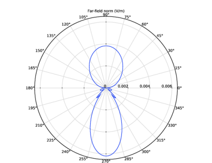
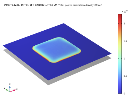
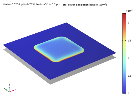
Click Replace Expression in the upper-right corner of the Expression section. From the menu, choose Component 1 (comp1) > Electromagnetic Waves, Frequency Domain 2 > Heating and losses > ewfd2.Qh - Total power dissipation density - W/m³.
Power Loss
1
Click the  Go to Default View button in the Graphics toolbar.
2
Click the  Zoom Extents button in the Graphics toolbar.
3
In the Model Builder window, click Power Loss.