|
|
|
|
1
|
|
2
|
In the Select Physics tree, select Optics > Wave Optics > Electromagnetic Waves, Frequency Domain (ewfd).
|
|
3
|
Click Add.
|
|
4
|
Click
|
|
5
|
In the Select Study tree, select Preset Studies for Selected Physics Interfaces > Wavelength Domain.
|
|
6
|
Click
|
|
1
|
|
2
|
|
1
|
|
2
|
|
3
|
|
1
|
|
2
|
|
3
|
|
4
|
|
5
|
Click
|
|
1
|
|
2
|
|
3
|
|
4
|
|
5
|
|
6
|
Click
|
|
1
|
|
2
|
|
3
|
|
4
|
|
5
|
Click
|
|
6
|
|
1
|
|
2
|
Click in the Graphics window and then press Ctrl+A to select all objects.
|
|
3
|
|
1
|
|
2
|
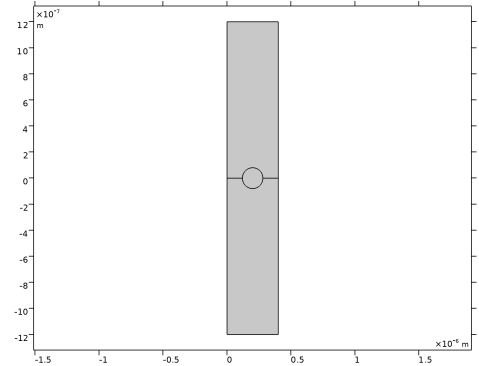
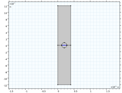
On the object uni1, select Boundary 6 only. This is the horizontal diameter of the circle in the center of the geometry.
 |
|
3
|
|
1
|
|
2
|
|
1
|
In the Model Builder window, under Component 1 (comp1) right-click Materials and choose Blank Material.
|
|
2
|
|
3
|
Locate the Material Contents section. In the table, enter the following settings:
|
|
1
|
|
2
|
|
4
|
Locate the Material Contents section. In the table, enter the following settings:
|
|
1
|
|
2
|
Go to the Add Material window.
|
|
3
|
In the tree, select Optical > Inorganic Materials > Au - Gold > Models and simulations > Au (Gold) (Rakic et al. 1998: Brendel-Bormann model; n,k 0.248-6.20 um), to select gold from the Optical material library.
|
|
4
|
Click the Add to Component button in the window toolbar.
|
|
5
|
|
1
|
In the Model Builder window, under Component 1 (comp1) click Electromagnetic Waves, Frequency Domain (ewfd).
|
|
2
|
|
3
|
|
1
|
|
2
|
|
3
|
|
4
|
Locate the Port Handling section. Click Add Diffraction Orders, to add Diffraction Order ports for the higher diffraction orders.
|
|
1
|
|
2
|
|
3
|
Select the Auxiliary sweep checkbox.
|
|
4
|
Click
|
|
6
|
Click
|
|
7
|
|
8
|
|
9
|
|
10
|
Click Replace.
|
|
11
|
|
13
|
|
1
|
|
2
|
In the Settings window for Arrow Line, click Replace Expression in the upper-right corner of the Expression section. From the menu, choose Component 1 (comp1) > Electromagnetic Waves, Frequency Domain > Ports > Wave vectors > ewfd.kIncx_1,ewfd.kIncy_1 - Incident wave vector.
|
|
3
|
|
4
|
Locate the Expression section.
|
|
5
|
|
6
|
|
7
|
Locate the Coloring and Style section.
|
|
8
|
|
1
|
|
1
|
In the Model Builder window, under Results > Electric Field (ewfd) right-click Arrow Line 1 and choose Duplicate.
|
|
2
|
In the Settings window for Arrow Line, click Replace Expression in the upper-right corner of the Expression section. From the menu, choose Component 1 (comp1) > Electromagnetic Waves, Frequency Domain > Ports > Wave vectors > ewfd.kModex_1,ewfd.kModey_1 - Port mode wave vector, port 1.
|
|
3
|
|
4
|
Locate the Expression section.
|
|
5
|
|
1
|
|
2
|
In the Settings window for Arrow Line, click Replace Expression in the upper-right corner of the Expression section. From the menu, choose Component 1 (comp1) > Electromagnetic Waves, Frequency Domain > Ports > Wave vectors > ewfd.kModex_2,ewfd.kModey_2 - Port mode wave vector, port 2.
|
|
3
|
|
4
|
Locate the Expression section.
|
|
5
|
|
1
|
|
2
|
|
3
|
Click
|
|
1
|
In the Model Builder window, under Results > Electric Field (ewfd) right-click Arrow Line 1 and choose Duplicate.
|
|
2
|
In the Settings window for Arrow Line, click Replace Expression in the upper-right corner of the Expression section. From the menu, choose Component 1 (comp1) > Electromagnetic Waves, Frequency Domain > Ports > Wave vectors > ewfd.kModex_3,ewfd.kModey_3 - Port mode wave vector, port 3.
|
|
3
|
|
4
|
Locate the Expression section.
|
|
5
|
|
1
|
|
2
|
In the Settings window for Arrow Line, click Replace Expression in the upper-right corner of the Expression section. From the menu, choose Component 1 (comp1) > Electromagnetic Waves, Frequency Domain > Ports > Wave vectors > ewfd.kModex_4,ewfd.kModey_4 - Port mode wave vector, port 4.
|
|
3
|
|
4
|
|
1
|
In the Model Builder window, under Results > Electric Field (ewfd) right-click Arrow Line 3 and choose Duplicate.
|
|
2
|
|
3
|
|
4
|
|
5
|
|
6
|
|
1
|
|
2
|
|
3
|
|
4
|
|
5
|
|
6
|
|
1
|
|
2
|
|
3
|
|
4
|
|
5
|
|
6
|
|
1
|
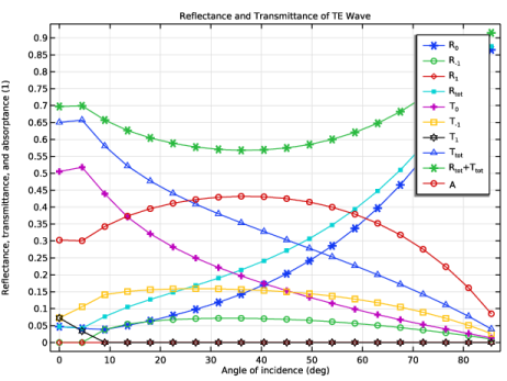
In the Model Builder window, under Results click Reflectance, Transmittance, and Absorptance (ewfd).
|
|
2
|
In the Settings window for 1D Plot Group, type TE Reflectance, Transmittance, and Absorptance in the Label text field.
|
|
3
|
|
4
|
|
1
|
In the Model Builder window, expand the TE Reflectance, Transmittance, and Absorptance node, then click Global 1.
|
|
2
|
|
3
|
|
4
|
|
6
|
|
1
|
In the Model Builder window, under Component 1 (comp1) click Electromagnetic Waves, Frequency Domain (ewfd).
|
|
2
|
|
3
|
|
1
|
|
2
|
Go to the Add Study window.
|
|
3
|
Find the Studies subsection. In the Select Study tree, select Preset Studies for Selected Physics Interfaces > Wavelength Domain.
|
|
4
|
Click the Add Study button in the window toolbar.
|
|
5
|
|
1
|
|
2
|
|
3
|
|
4
|
Click
|
|
6
|
Click
|
|
7
|
|
8
|
|
9
|
|
10
|
Click Replace.
|
|
11
|
|
13
|
|
1
|
|
2
|
In the Settings window for Arrow Line, click Replace Expression in the upper-right corner of the Expression section. From the menu, choose Component 1 (comp1) > Electromagnetic Waves, Frequency Domain > Ports > Wave vectors > ewfd.kIncx_1,ewfd.kIncy_1 - Incident wave vector.
|
|
3
|
|
4
|
Locate the Expression section.
|
|
5
|
|
6
|
|
7
|
Locate the Coloring and Style section.
|
|
8
|
|
1
|
|
1
|
In the Model Builder window, under Results > Electric Field (ewfd) right-click Arrow Line 1 and choose Duplicate.
|
|
2
|
In the Settings window for Arrow Line, click Replace Expression in the upper-right corner of the Expression section. From the menu, choose Component 1 (comp1) > Electromagnetic Waves, Frequency Domain > Ports > Wave vectors > ewfd.kModex_1,ewfd.kModey_1 - Port mode wave vector, port 1.
|
|
3
|
|
4
|
Locate the Expression section.
|
|
5
|
|
1
|
|
2
|
In the Settings window for Arrow Line, click Replace Expression in the upper-right corner of the Expression section. From the menu, choose Component 1 (comp1) > Electromagnetic Waves, Frequency Domain > Ports > Wave vectors > ewfd.kModex_2,ewfd.kModey_2 - Port mode wave vector, port 2.
|
|
3
|
|
4
|
Locate the Expression section.
|
|
5
|
|
1
|
|
2
|
|
3
|
Click
|
|
1
|
In the Model Builder window, under Results > Electric Field (ewfd) right-click Arrow Line 1 and choose Duplicate.
|
|
2
|
In the Settings window for Arrow Line, click Replace Expression in the upper-right corner of the Expression section. From the menu, choose Component 1 (comp1) > Electromagnetic Waves, Frequency Domain > Ports > Wave vectors > ewfd.kModex_3,ewfd.kModey_3 - Port mode wave vector, port 3.
|
|
3
|
|
4
|
Locate the Expression section.
|
|
5
|
|
1
|
|
2
|
In the Settings window for Arrow Line, click Replace Expression in the upper-right corner of the Expression section. From the menu, choose Component 1 (comp1) > Electromagnetic Waves, Frequency Domain > Ports > Wave vectors > ewfd.kModex_4,ewfd.kModey_4 - Port mode wave vector, port 4.
|
|
3
|
|
4
|
|
1
|
In the Model Builder window, under Results > Electric Field (ewfd) right-click Arrow Line 3 and choose Duplicate.
|
|
2
|
|
3
|
|
4
|
|
5
|
|
6
|
|
1
|
|
2
|
|
3
|
|
4
|
|
5
|
|
6
|
|
1
|
|
2
|
|
3
|
|
4
|
|
5
|
|
6
|
|
1
|
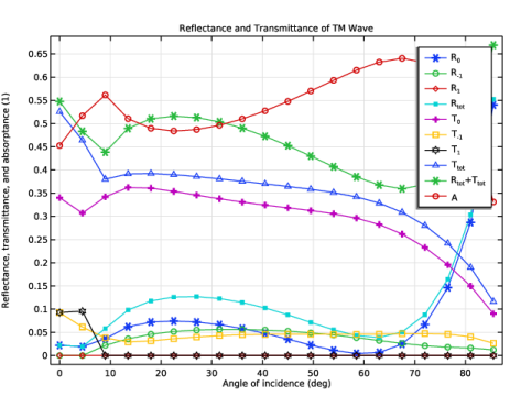
In the Model Builder window, under Results click Reflectance, Transmittance, and Absorptance (ewfd).
|
|
2
|
In the Settings window for 1D Plot Group, type TM Reflectance, Transmittance, and Absorptance in the Label text field.
|
|
3
|
|
4
|
|
1
|
In the Model Builder window, expand the TM Reflectance, Transmittance, and Absorptance node, then click Global 1.
|
|
2
|
|
3
|
|
4
|