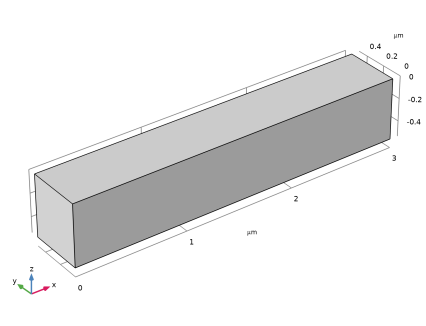
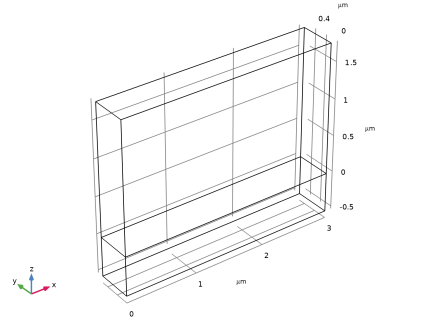
PDF

Metasurface Beam Deflector
Introduction
Structured arrays of metamaterial elements can control electromagnetic waves in exotic ways. As a specific example of this, Ref. 1, the traditional form of Snell’s law was modified to include a phase gradient at the interface between two media. For transmission, this generalized Snell’s law takes the form
(1)
Using this generalized form, the transmitted angle, θt, can be expressed as a function of both the incident angle, θi, and the phase function, ϕ, at the interface. If the right-hand side of the equation is zero, we regain the traditional form of Snell’s law. This is called ordinary refraction and the newly allowed transmission angles are referred to as anomalous refraction.
Figure 1: Ordinary and anomalous reflection and refraction angles from a metasurface.
Because individual metamaterial elements are typically subwavelength, they can be used to design an effective phase function ϕ(r) and control the reflected and refracted light. When metamaterial elements are arrayed on an interface, they are often referred to as a metasurface.
Model Definition
In this model we demonstrate how to simulate a metasurface beam deflector that demonstrates anomalous refraction. The structure itself is a repeated array of six meta elements shown in Figure 2. The periodicity of the individual elements is 500 nm, and so the full structure of six elements is 3 μm wide. The posts are 1 μm tall, and the structure is designed to operate at a free-space wavelength of 1.55 μm.
Figure 2: μm tall silicon posts on a SiO2 substrate. The periodicity of the individual elements is 500 nm, and so the full structure of six elements is 3 μm wide.
The cylindrical pillars are silicon and the substrate is SiO2. The structure is designed so that incident light coming through the substrate at a normal angle of incidence will be refracted at prescribed angle. Because of the periodicity of the overall structure, the grating equation can be used to determine the possible angles for transmitted waves:
(2)
The diffraction order is m, and d is the grating distance of 3 μm. For a normal angle of incidence, the angle of the first refracted mode will be 31.1 degrees (θ = arcsin(λ/d)). This corresponds with a linear phase function that varies from 0 to 2π across the unit cell ϕ(x) = 2πx/d. The radii of the six cylindrical posts have been chosen to approximate this phase shift.
To define the periodic unit cell, a Periodic Structure node is used. This node automatically adds and configures Floquet Periodic Condition nodes in the x and y directions, combined with Periodic Ports in the z direction. The Diffraction Order subnodes on the Periodic Ports will fully account for the transmission and reflection into each allowed diffraction direction.
Results and Discussion
The incident wave is polarized in the y direction, and Figure 3 shows the results of Ey for an array of three full unit cells.
Figure 3: The electric field in the y direction for an array of 3 unit cells. Notice that the electric field wavefronts at the bottom of the structure are approximately horizontal, while the wavefronts at the top have been deflected to the right at approximately 31 degrees.
By comparing the wave fronts at the top and bottom of the structure, we can qualitatively observe that the desired behavior of deflecting a normally incident wave has been achieved. We can also notice that the pillars having a large radius provide more phase accumulation than smaller radius pillars. This makes intuitive sense if we consider the limiting behavior of a wave propagating through a homogeneous domain of either air or Si. The phase accumulation in those trivial cases will simply be ϕ tPostnk0, where n is the material index and tPost is the structure height. The actual response of the posts is substantially more complex than this naïve picture, and requires simulation to fully capture, but this picture does yield insight into the rough behavior of the structure as there is more or less air vs Si in the six meta elements.
A more quantitative evaluation of the device is given by the transmittance values. The desired transmission mode has a transmittance value of T = 0.85. The combined transmittance and reflectance of all orders, respectively, is 0.88 and 0.12 clearly indicating that the structure is routing the beam as designed.
The device could be further optimized to maximize the transmittance of the desired mode. This is relevant because the current design was created using a standard approach called the locally periodic approximation. In the locally periodic approximation, the phase response of each individual pillar is determined by simulating an infinite array of identical elements. As the six elements in the beam deflector are clearly not identical, optimization could enhance the performance of this initial design.
Reference
1. N. Yu and others, “Light Propagation with Phase Discontinuities: Generalized Laws of Reflection and Refraction,” Science, vol. 334, pp. 333–337, 2011. DOI: doi.org/10.1126/science.1210713.
Application Library path: Wave_Optics_Module/Gratings_and_Metamaterials/metasurface_beam_deflector
Modeling Instructions
From the File menu, choose New.
New
In the New window, click  Model Wizard.
Model Wizard
1
In the Model Wizard window, click  3D.
2
In the Select Physics tree, select Optics > Wave Optics > Electromagnetic Waves, Frequency Domain (ewfd).
3
Click Add.
4
Click  Study.
5
In the Select Study tree, select Preset Studies for Selected Physics Interfaces > Wavelength Domain.
6
Global Definitions
Parameters 1
1
In the Model Builder window, under Global Definitions click Parameters 1.
2
In the Settings window for Parameters, locate the Parameters section.
3
Click  Load from File.
4
The loaded parameters defines the wavelength and the dimensions of the geometry.
Geometry 1
Start by building the geometry.
1
In the Model Builder window, under Component 1 (comp1) click Geometry 1.
2
In the Settings window for Geometry, locate the Units section.
3
From the Length unit list, choose µm.
Substrate
1
In the Geometry toolbar, click  Block.
2
In the Settings window for Block, type Substrate in the Label text field.
3
Locate the Size and Shape section. In the Width text field, type d.
4
In the Depth text field, type py.
5
In the Height text field, type tSub.
6
Locate the Position section. In the z text field, type -tSub.
7
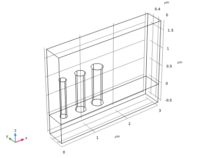
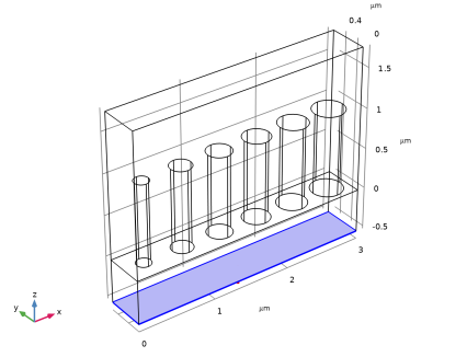
Locate the Selections of Resulting Entities section. Select the Resulting objects selection checkbox, to generate a domain selection named Substrate.
8
Click  Build Selected.
Air Block
1
Right-click Substrate and choose Duplicate.
2
In the Settings window for Block, type Air Block in the Label text field.
3
Locate the Size and Shape section. In the Height text field, type tAir.
4
Locate the Position section. In the z text field, type 0.
5
Locate the Selections of Resulting Entities section. From the Show in physics list, choose Off.
6
Click the  Wireframe Rendering button in the Graphics toolbar.
7
In the Geometry toolbar, click  Build All.
8
Click the  Zoom Extents button in the Graphics toolbar. This will make it easier to see the posts that will be added in the next steps.
9
In the Model Builder window, click Geometry 1.
Post 1
1
In the Geometry toolbar, click  Cylinder.
2
In the Settings window for Cylinder, type Post 1 in the Label text field.
3
Locate the Size and Shape section. In the Radius text field, type r1.
4
In the Height text field, type tPost.
5
Locate the Position section. In the x text field, type x1.
6
In the y text field, type py/2.
7
Locate the Selections of Resulting Entities section. Find the Cumulative selection subsection. Click New.
8
In the New Cumulative Selection dialog, type Posts in the Name text field.
9
10
In the Settings window for Cylinder, click  Build Selected.
Post 2
1
Right-click Post 1 and choose Duplicate.
2
In the Settings window for Cylinder, type Post 2 in the Label text field.
3
Locate the Size and Shape section. In the Radius text field, type r2.
4
Locate the Position section. In the x text field, type x2.
5
Click  Build Selected.
Post 3
1
Right-click Post 2 and choose Duplicate.
2
In the Settings window for Cylinder, type Post 3 in the Label text field.
3
Locate the Size and Shape section. In the Radius text field, type r3.
4
Locate the Position section. In the x text field, type x3.
5
Click  Build Selected.
Post 4
1
Right-click Post 3 and choose Duplicate.
2
In the Settings window for Cylinder, type Post 4 in the Label text field.
3
Locate the Size and Shape section. In the Radius text field, type r4.
4
Locate the Position section. In the x text field, type x4.
5
Click  Build Selected.
Post 5
1
Right-click Post 4 and choose Duplicate.
2
In the Settings window for Cylinder, type Post 5 in the Label text field.
3
Locate the Size and Shape section. In the Radius text field, type r5.
4
Locate the Position section. In the x text field, type x5.
5
Click  Build Selected.
Post 6
1
Right-click Post 5 and choose Duplicate.
2
In the Settings window for Cylinder, type Post 6 in the Label text field.
3
Locate the Size and Shape section. In the Radius text field, type r6.
4
Locate the Position section. In the x text field, type x6.
5
Click  Build Selected.
Air
1
In the Geometry toolbar, click  Selections and choose Difference Selection.
2
In the Settings window for Difference Selection, type Air in the Label text field.
3
Locate the Input Entities section. Click the  Add button for Selections to add.
4
In the Add dialog, select Air Block in the Selections to add list.
5
6
In the Settings window for Difference Selection, locate the Input Entities section.
7
Click the  Add button for Selections to subtract.
8
In the Add dialog, select Posts in the Selections to subtract list.
9
10
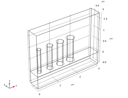
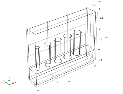
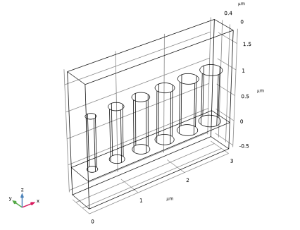
Drag and drop below Form Union (fin), to generate a domain where the posts are subtracted from the air block.
11
In the Geometry toolbar, click  Build All.
Now, the geometry is built and the materials can be added.
Add Material
1
In the Materials toolbar, click  Add Material to open the Add Material window.
2
Go to the Add Material window.
3
In the tree, select Optical > Inorganic Materials > Si - Silicon, silicides and silicates > Amorphous silicon (α-Si) > Si (Silicon) (Pierce and Spicer 1972: a-Si; n,k 0.0103-2.07 um).
4
Click the Add to Component button in the window toolbar.
5
In the tree, select Optical > Inorganic Materials > O - Oxygen and oxides > Fused silica > SiO2 (Silicon dioxide, Silica, Quartz) (Malitson 1965: Fused silica; n 0.21-6.7 um).
6
Click the Add to Component button in the window toolbar.
Materials
SiO2 (Silicon dioxide, Silica, Quartz) (Malitson 1965: Fused silica; n 0.21-6.7 um) (mat2)
1
In the Settings window for Material, locate the Geometric Entity Selection section.
2
From the Selection list, choose Substrate.
Air
1
In the Model Builder window, right-click Materials and choose Blank Material.
2
In the Settings window for Material, type Air in the Label text field.
3
Locate the Geometric Entity Selection section. From the Selection list, choose Air.
4
Locate the Material Contents section. In the table, enter the following settings:
5
In the Materials toolbar, click  Add Material to close the Add Material window, to make more space for the Graphics window.
Study 1
Step 1: Wavelength Domain
1
In the Settings window for Wavelength Domain, locate the Study Settings section.
2
In the Wavelengths text field, type lda0.
Electromagnetic Waves, Frequency Domain (ewfd)
Periodic Structure 1
1
In the Physics toolbar, click  Domains and choose Periodic Structure.
2
In the Settings window for Periodic Structure, locate the Excited Port Selection section.
3
Click to select the  Activate Selection toggle button.
4
5
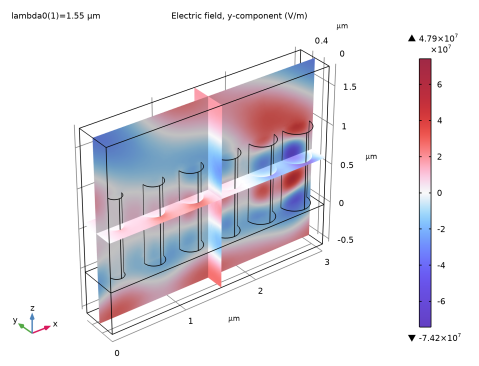
Locate the Port Handling section. From the Diffraction order specification list, choose From current parameters, as only normal incidence will be considered in this model.
6
Click Add Diffraction Orders, to automatically generate the diffraction orders for both ports.
Study 1
In the Study toolbar, click  Compute.
Results
Multislice 1
1
In the Model Builder window, expand the Electric Field (ewfd) node, then click Multislice 1.
2
In the Settings window for Multislice, locate the Expression section.
3
In the Expression text field, type ewfd.Ey.
4
Locate the Coloring and Style section. From the Color table list, choose WaveLight.
5
From the Scale list, choose Linear symmetric.
6
In the Electric Field (ewfd) toolbar, click  Plot.
7
Click the  Zoom Extents button in the Graphics toolbar.
The y component is the dominant polarization.
Polarization Plot (ewfd)
1
In the Model Builder window, under Results click Polarization Plot (ewfd).
This plot verifies that only the modes m = n = 0, m = ±1, n = 0, and m = ±2, n = 0 should be added to the excitation (reflection) side and the modes m = n = 0 and m = ±1, n = 0 should be added to the transmission side.
Array 3D 1
Finally, add a plot with three adjacent cells of the y component of the electric field.
1
In the Results toolbar, click  More Datasets and choose Array 3D.
2
In the Settings window for Array 3D, locate the Array Size section.
3
In the X size text field, type 3.
4
Click to expand the Advanced section. Select the Floquet–Bloch periodicity checkbox.
5
Find the Wave vector subsection. In the X text field, type ewfd.kPeriodicx.
Ey in Array
1
In the Results toolbar, click  3D Plot Group.
2
In the Settings window for 3D Plot Group, type Ey in Array in the Label text field.
3
Locate the Data section. From the Dataset list, choose Array 3D 1.
4
Click to expand the Title section. From the Title type list, choose None.
Slice 1
1
Right-click Ey in Array and choose Slice.
2
In the Settings window for Slice, locate the Expression section.
3
In the Expression text field, type ewfd.Ey.
4
Locate the Plane Data section. From the Plane list, choose zx-planes.
5
In the Planes text field, type 1.
6
Locate the Coloring and Style section. From the Color table list, choose WaveLight.
7
From the Scale list, choose Linear symmetric.
8
In the Ey in Array toolbar, click  Plot.
9
Click the  Go to XZ View button in the Graphics toolbar.
10
Click the  Show Legends button in the Graphics toolbar.
11
Click the  Show Grid button in the Graphics toolbar.
12
Click the  Show Axis Orientation button in the Graphics toolbar.
13
Click the  Zoom Extents button in the Graphics toolbar.
Animation 1
1
In the Ey in Array toolbar, click  Animation and choose Player.
2
In the Settings window for Animation, locate the Animation Editing section.
3
From the Sequence type list, choose Dynamic data extension.
4
Locate the Playing section. From the Repeat list, choose Number of iterations.
5
In the Number of iterations text field, type 5.
6
Click the  Play button in the Graphics toolbar.
Notice the normally incident plane wave, coming from below, and the refracted almost plane wave above the structure.