PDF

Simulation of Metal–Air Surface Plasmon Polariton Propagation and Dispersion
Introduction
Electromagnetic waves that are confined to propagate along a surface, such as surface plasmon polaritons (SPPs), are of great research interest due to their potential applications in nanoscale manipulation of light. This model will discuss how to set up a simulation to visualize the propagation as well as the frequency versus propagation constant dispersion relationship of SPPs.
Propagating electromagnetic waves can exist in a variety of forms — such as plane waves, spherical waves, Gaussian beams, and so on. There are also propagating electromagnetic waves that are confined in space, such as waveguide modes propagating in metallic or dielectric waveguides.
In addition, there is another special type of electromagnetic wave that is confined to a planar surface. This type of wave propagates tangentially to the surface with exponentially decaying fields in the perpendicular direction. Its wavelength is often smaller than the free space wavelength at the same frequency. Thus, this type of wave provides promises for nanoscale control and manipulation of photons, which is desirable in many applications, ranging from optical communication and information processing to solar energy harvesting and digital displays.
The existence of this wave type was found at metal–dielectric interfaces and is known as surface plasmon polariton. The term plasmon refers to the collective oscillation of charges in a metal, whereas the term polariton generally refers to a quasi-particle that is the result of the coupling between a photon with a polar excitation in a material. The SPPs are the result of coupling of surface plasmons and light.
Model Definition
This model demonstrates SPPs in the simplest system that supports it, namely the bulk metal–dielectric interface. Imagine that the metal–dielectric interface is represented by the xz plane at y = 0. The dielectric region is above the plane, y > 0, and the metal region is below the plane, y < 0. The surface wave propagates in the x direction.
Figure 1: A metal–dielectric interface at y = 0. In this model, the SPP propagates in the x direction and exponentially decays in the y direction.
Here, it is of interest to study a TM mode surface wave. The expressions for the electric and magnetic fields in the dielectric and the metal are then given by
(1)
(2)
(3)
(4)
where the d and m superscripts denote quantities in dielectric and metallic domains, respectively. β is the complex SPP propagation constant. Both γd and γm are positive real numbers that describe the decay of the field away from the metal–dielectric interface.
The tangential components of the electric and magnetic fields, and the normal component of the electric displacement field, are continuous across the metal–dielectric boundary. Therefore,
(5)
(6)
(7).
Since there is no external charge and the permittivity is constant inside the respective metallic and dielectric domains, ∇⋅E = 0 must hold inside the two regions. Combining this condition with Equation 2 and Equation 4, gives the following two equations
(8)
(9).
Subsequently, if those two equations are combined, you get the simple relation
(10).
From this relation, it is clear why SPPs only exist between a dielectric, having a positive real part of the permittivity, and a metal, having a negative real part of the permittivity. To have the field decay in the y direction, both γd and γm must be positive, which means that the permittivities εd and εm must have opposite signs.
To derive the expression for the propagation constant β, the Helmholtz equation is used
(11),
where k0 = ω/c is the free space wave number.Plugging Equation 2 and Equation 4 into the Helmholtz equation leads to
(12)
(13).
Finally, combining Equation 10, Equation 12, and Equation 13, the following expression for the SPP propagation constant is derived
(14).
The real part of β is related to the SPP wavelength by λSPP = 2π/Re(β), while the imaginary part describes the SPP propagation loss. Generally, the permittivities εd and εm are frequency dependent, so β is also frequency-dependent. The relationship between β and the frequency is often what needs to be known to characterize the SPPs in a system.
Remember that the above discussion is purely based on the assumption that the SPP is a TM wave. For the possibility of the TE wave, one can simply follow the previous derivation steps and show that all the field amplitudes must be zero. This means that SPPs only exist as a TM wave.
This model simulates SPPs propagating at the interface between silver (metal) and air (dielectric), using material properties for silver from the built-in Optical Material Library. Numeric ports are used on the left and right boundaries of the model. The left port, with excitation turned on, will launch the SPP, while the right port, with excitation turned off, will absorb the SPP without reflection. To get the mode field for both ports, two Boundary Mode Analysis study steps are added. Finally, a Frequency Domain study step is used when solving for the domain field.
Results and Discussion
Figure 2 shows the wave as it propagates in the x direction. The decay in the y direction is faster on the metal side due to the strong absorption.
Figure 2: The y-component of the electric field for a wavelength of 370 nm (3.35 eV). The wave gets weaker, due to absorption, as it propagates from left to right. The arrows indicate the electric field strength and direction.
Figure 3 confirms that there is strong absorption for short wavelengths, whereas for longer wavelengths the transmission increases.
Figure 3: A plot of the transmittance and absorptance versus wavelength.
The mode field plot in Figure 4 clearly shows that the SPP decays much faster in the silver domain than in the air domain.
Figure 4: The norm of the electric mode field for Port 1.
To capture the quantitative relationship between the frequency (photon energy) and β, a plot of freq*h_const on the y-axis versus the propagation constant ewfd.beta_1 on the x-axis (shown by the circle markers) is shown in Figure 5.
When studying SPPs, it is customary to define a figure of merit, often referred to as the Q factor, as the ratio of the real and the imaginary part of β. When β has a smaller imaginary part (equivalently, a larger Q factor), the SPP can propagate a long distance relative to its wavelength before it is attenuated. A larger Q factor is usually desirable for practical applications. The Q factor can conveniently be plotted using a color expression added to the dispersion curve. Here, a brighter color represents higher Q factors and a darker color represents lower Q factors. In addition, a dashed line representing f = c, often called the light line, is added. The light line is the dispersion relation of free space photons. Lastly, the analytical expression from Equation 13 is plotted as a solid curve. The simulated dispersion and the analytical expression show good agreement.
The dispersion plot in Figure 5 is very representative for the SPP dispersion in noble metals. This plot is useful for gaining insight of the characteristics of SPPs. More importantly, it shows that the dispersion curve of SPPs always lies on the right side of the light line. The implication of this is that the SPP wavelength is always smaller than the wavelength of free space waves. This is why SPPs can be used as a way to compress the wavelength of light to achieve a higher field concentration.
Furthermore, the mismatch between the free-space wave number and the SPP propagation constant means that it is not possible to excite SPPs simply by shining light onto the metal surface. Some external mechanism to achieve phase matching is required. The excitation of SPPs is often done using total internal reflection from a prism or using diffraction from a grating. The goal of with these techniques is to prepare the electromagnetic field, so that its propagation constant matches that of the SPP at the same frequency.
Figure 5: A plot of the simulated dispersion curve of the SPP at the interface between silver and air. The simulated result (circles) is consistent with the analytical calculation (solid line). The free space light dispersion, or light line, is represented by a dashed line. The color represents the Q factor of SPP.
For more SPP simulation examples, see the blog post in Ref. 1.
Reference
1. X. Chen, “Modeling Surface Plasmon Polaritons in COMSOL®,” COMSOL Blog, 12 Oct. 2022; www.comsol.com/blogs/modeling-surface-plasmon-polaritons-in-comsol/.
Application Library path: Wave_Optics_Module/Waveguides/metal_air_surface_plasmon_polariton
Modeling Instructions
From the File menu, choose New.
New
In the New window, click  Model Wizard.
Model Wizard
1
In the Model Wizard window, click  2D.
2
In the Select Physics tree, select Optics > Wave Optics > Electromagnetic Waves, Frequency Domain (ewfd).
3
Click Add.
4
Click  Study.
5
In the Select Study tree, select Preset Studies for Selected Physics Interfaces > Boundary Mode Analysis.
6
Global Definitions
Parameters 1
1
In the Model Builder window, under Global Definitions click Parameters 1.
2
In the Settings window for Parameters, locate the Parameters section.
3
The constant c_const above represents the speed of light.
Geometry 1
The geometry is very simple, consisting of only one rectangle that is split into two halves.
1
In the Model Builder window, under Component 1 (comp1) click Geometry 1.
2
In the Settings window for Geometry, locate the Units section.
3
From the Length unit list, choose nm.
Rectangle 1 (r1)
1
In the Geometry toolbar, click  Rectangle.
2
In the Settings window for Rectangle, locate the Size and Shape section.
3
In the Width text field, type L.
4
In the Height text field, type H.
5
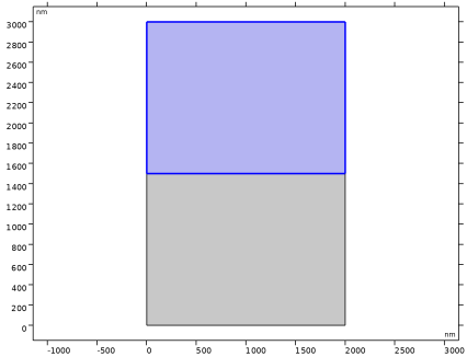
Click to expand the Layers section. In the table, enter the following settings:
6
Click  Build All Objects.
Materials
Pick silver from the Optical material library.
Add Material
1
In the Materials toolbar, click  Add Material to open the Add Material window.
2
Go to the Add Material window.
3
In the tree, select Optical > Inorganic Materials > Ag - Silver > Experimental data: bulk, thick film > Ag (Silver) (Johnson and Christy 1972: n,k 0.188-1.94 um).
4
Click the Add to Component button in the window toolbar.
Materials
Air
1
In the Model Builder window, under Component 1 (comp1) right-click Materials and choose Blank Material.
2
In the Settings window for Material, type Air in the Label text field.
3
4
Locate the Material Contents section. In the table, enter the following settings:
5
In the Materials toolbar, click  Add Material to close the Add Material window.
Electromagnetic Waves, Frequency Domain (ewfd)
Port 1
1
In the Physics toolbar, click  Boundaries and choose Port.
2
3
In the Settings window for Port, locate the Port Properties section.
4
From the Type of port list, choose Numeric.
Port 2
1
In the Physics toolbar, click  Boundaries and choose Port.
2
3
In the Settings window for Port, locate the Port Properties section.
4
From the Type of port list, choose Numeric.
Study 1
Step 1: Boundary Mode Analysis
1
In the Model Builder window, under Study 1 click Step 1: Boundary Mode Analysis.
2
In the Settings window for Boundary Mode Analysis, locate the Study Settings section.
3
In the Mode analysis frequency text field, type f0.
4
Select the Search for modes around shift checkbox. In the associated text field, type 5.
Step 3: Boundary Mode Analysis 1
1
Right-click Study 1 > Step 1: Boundary Mode Analysis and choose Duplicate.
2
Right-click Step 3: Boundary Mode Analysis 1 and choose Move Up.
3
In the Settings window for Boundary Mode Analysis, locate the Study Settings section.
4
In the Port name text field, type 2.
Step 3: Frequency Domain
1
In the Model Builder window, click Step 3: Frequency Domain.
2
In the Settings window for Frequency Domain, locate the Study Settings section.
3
In the Frequencies text field, type f0.
Parametric Sweep
1
In the Study toolbar, click  Parametric Sweep.
2
In the Settings window for Parametric Sweep, locate the Study Settings section.
3
4
5
Click  Range.
6
In the Range dialog, type 340 in the Start text field.
7
In the Step text field, type 10.
8
In the Stop text field, type 600.
9
Click Add.
Definitions
Analytic 1 (an1)
1
In the Definitions toolbar, click  Analytic.
2
In the Settings window for Analytic, type epsilonr in the Function name text field.
3
Locate the Definition section. In the Expression text field, type (mat1.rfi.nr(x)-1i*mat1.rfi.ni(x))^2.
4
Click to expand the Advanced section. Select the May produce complex output for real arguments checkbox.
This analytical function calculates the relative permittivity of silver.
Mesh 1
1
In the Model Builder window, under Component 1 (comp1) right-click Mesh 1 and choose Build All.
2
In the Settings window for Mesh, locate the Sequence Type section.
3
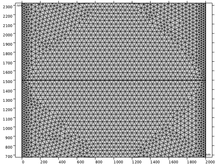
From the list, choose User-controlled mesh.
Size 2
1
Right-click Component 1 (comp1) > Mesh 1 and choose Size.
2
Drag and drop Size 2 below Size 1.
3
In the Settings window for Size, locate the Geometric Entity Selection section.
4
From the Geometric entity level list, choose Boundary.
5
6
Locate the Element Size section. Click the Custom button.
7
Locate the Element Size Parameters section.
8
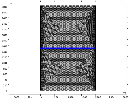
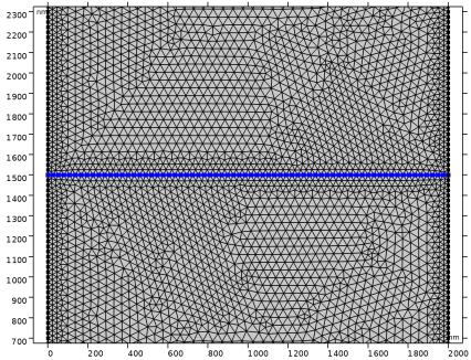
Select the Maximum element size checkbox. In the associated text field, type (lda0/real(sqrt(epsilonr(lda0/1[m])/(1+epsilonr(lda0/1[m])))))/12.
The maximum element size should be much smaller than SPP wavelength.
9
Click  Build All.
The mesh at the metal-air interface is finer than the one built using Physics-controlled mesh.
Study 1
In the Study toolbar, click  Compute.
Results
Electric Field (ewfd)
1
In the Settings window for 2D Plot Group, locate the Data section.
2
From the Parameter value (lda0 (nm)) list, choose 370.
3
In the Electric Field (ewfd) toolbar, click  Plot.
Surface 1
1
In the Model Builder window, expand the Electric Field (ewfd) node, then click Surface 1.
2
In the Settings window for Surface, locate the Expression section.
3
In the Expression text field, type ewfd.Ey.
4
Locate the Coloring and Style section. From the Color table list, choose WaveLight.
5
From the Scale list, choose Linear symmetric.
Arrow Surface 1
1
In the Model Builder window, right-click Electric Field (ewfd) and choose Arrow Surface.
2
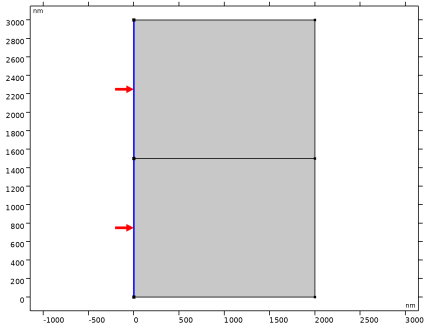
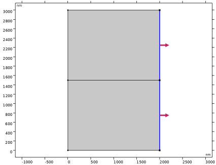
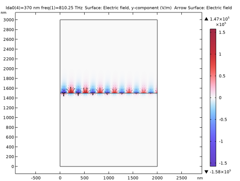
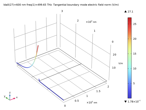
In the Settings window for Arrow Surface, click Replace Expression in the upper-right corner of the Expression section. From the menu, choose Component 1 (comp1) > Electromagnetic Waves, Frequency Domain > Electric > ewfd.Ex,ewfd.Ey - Electric field.
3
Locate the Arrow Positioning section. Find the X grid points subsection. In the Points text field, type 50.
4
Find the Y grid points subsection. In the Points text field, type 50.
5
Locate the Coloring and Style section. From the Color list, choose Black.
6
In the Electric Field (ewfd) toolbar, click  Plot.
7
Select the Scale factor checkbox. In the associated text field, type 1e-3.
Transmittance and Absorptance (ewfd)
Before creating the frequency versus propagation constant dispersion plot, it is good to inspect some of the default plots that are automatically generated when performing a simulation with Numeric ports.
The reflectance is small and not of interest here. So, curves related to the reflectance will be removed from the plot.
1
In the Model Builder window, under Results click Reflectance, Transmittance, and Absorptance (ewfd).
2
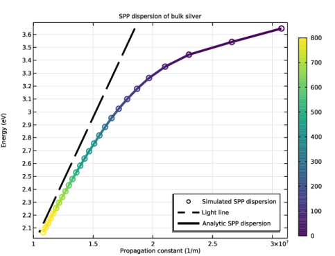
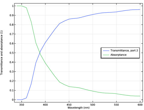
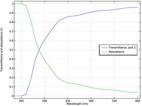
In the Settings window for 1D Plot Group, type Transmittance and Absorptance (ewfd) in the Label text field.
3
Locate the Plot Settings section. In the y-axis label text field, type Transmittance and absorptance (1).
4
Locate the Legend section. From the Position list, choose Middle right.
Global 1
1
In the Model Builder window, expand the Transmittance and Absorptance (ewfd) node, then click Global 1.
2
In the Settings window for Global, locate the y-Axis Data section.
3
4
Click  Delete.
5
In the Transmittance and Absorptance (ewfd) toolbar, click  Plot.
This figure shows that the absorption is large for short wavelengths and falls off to low values for longer wavelengths.
Electric Mode Field, Port 1 (ewfd)
1
In the Model Builder window, under Results click Electric Mode Field, Port 1 (ewfd).
This figure shows the electric mode field norm for Port 1. It is clear that the wave decays rapidly in the metal and is extending more into the dielectric domain.
SPP Dispersion
1
In the Results toolbar, click  1D Plot Group.
2
In the Settings window for 1D Plot Group, type SPP Dispersion in the Label text field.
3
Locate the Data section. From the Dataset list, choose Study 1/Parametric Solutions 1 (sol4).
4
Click to expand the Title section. From the Title type list, choose Manual.
5
In the Title text area, type SPP dispersion of bulk silver.
6
Locate the Plot Settings section.
7
Select the x-axis label checkbox. In the associated text field, type Propagation constant (1/m).
8
Locate the Legend section. From the Position list, choose Lower right.
Global 1
1
Right-click SPP Dispersion and choose Global.
2
In the Settings window for Global, locate the y-Axis Data section.
3
4
Locate the x-Axis Data section. From the Axis source data list, choose All solutions.
5
From the Parameter list, choose Expression.
6
In the Expression text field, type ewfd.beta_1.
7
Click to expand the Coloring and Style section. Find the Line style subsection. From the Line list, choose None.
8
From the Width list, choose 3.
9
Find the Line markers subsection. From the Marker list, choose Circle.
10
Click to expand the Legends section. From the Legends list, choose Manual.
11
Global 2
1
Right-click Global 1 and choose Duplicate.
2
In the Settings window for Global, locate the x-Axis Data section.
3
In the Expression text field, type ewfd.k0.
4
Locate the Coloring and Style section. Find the Line style subsection. From the Line list, choose Dashed.
5
From the Color list, choose Black.
6
Find the Line markers subsection. From the Marker list, choose None.
7
Locate the Legends section. In the table, enter the following settings:
Color Expression 1
1
In the Model Builder window, right-click Global 1 and choose Color Expression.
2
In the Settings window for Color Expression, locate the Expression section.
3
In the Expression text field, type -real(ewfd.beta_1)/imag(ewfd.beta_1).
4
Locate the Coloring and Style section. From the Color table list, choose Viridis.
5
Click to expand the Range section. Select the Manual color range checkbox.
6
In the Minimum text field, type 0.
7
In the Maximum text field, type 800.
Global 3
1
Right-click Global 1 and choose Duplicate.
2
In the Settings window for Global, locate the x-Axis Data section.
3
In the Expression text field, type ewfd.omega/c_const*sqrt(epsilonr(lda0)/(epsilonr(lda0)+1)).
4
Locate the Coloring and Style section. Find the Line style subsection. From the Line list, choose Solid.
5
From the Width list, choose 4.
6
Find the Line markers subsection. From the Marker list, choose None.
7
Locate the Legends section. In the table, enter the following settings:
Color Expression 1
1
In the Model Builder window, expand the Global 3 node, then click Color Expression 1.
2
In the Settings window for Color Expression, locate the Expression section.
3
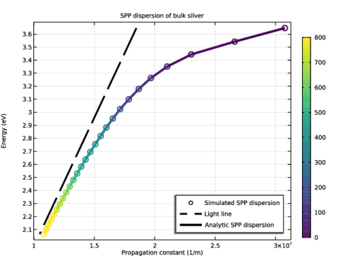
In the Expression text field, type real((ewfd.omega/c_const)*sqrt(epsilonr(lda0)/(epsilonr(lda0)+1)))/imag(-(ewfd.omega/c_const)*sqrt(epsilonr(lda0)/(epsilonr(lda0)+1))).
4
Locate the Coloring and Style section. Clear the Color legend checkbox.
5
In the SPP Dispersion toolbar, click  Plot.