|
|
|

|
1
|
|
2
|
In the Select Physics tree, select Optics > Wave Optics > Electromagnetic Waves, Frequency Domain (ewfd).
|
|
3
|
Click Add.
|
|
4
|
Click
|
|
5
|
In the Select Study tree, select Preset Studies for Selected Physics Interfaces > Wavelength Domain.
|
|
6
|
Click
|
|
1
|
|
2
|
|
1
|
|
2
|
|
3
|
Click
|
|
4
|
|
5
|
|
6
|
|
7
|
Click Replace.
|
|
1
|
|
2
|
|
3
|
|
1
|
|
2
|
|
1
|
|
2
|
|
1
|
|
2
|
|
1
|
|
2
|
|
3
|
|
1
|
|
2
|
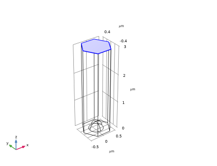
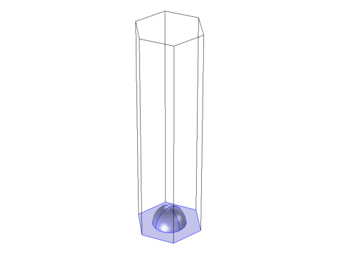
Select the object ext1 only.
|
|
3
|
|
4
|
|
5
|
Select the object sph1 only.
|
|
6
|
Click
|
|
7
|
|
8
|
|
1
|
|
2
|
Go to the Add Material window.
|
|
3
|
|
4
|
Click the Add to Component button in the window toolbar.
|
|
5
|
|
1
|
|
2
|
|
3
|
Clear the Add listener port checkbox, as the bottom boundary should use the default Perfect Electric Conductor 1 node.
|
|
4
|
|
5
|
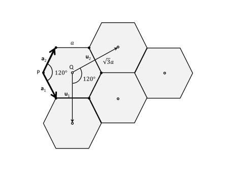
In the α2 text field, type phi, as this angle is measured from the Reference Direction subnode of the Periodic Structure.
|
|
6
|
|
7
|
Locate the Port Handling section. From the Diffraction order specification list, choose From current parameters, as no angle sweep will be done in this example model.
|
|
8
|
Click Add Diffraction Orders.
|
|
1
|
|
2
|
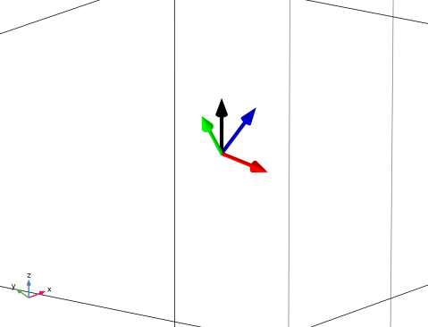
In the Settings window for Arrow Surface, click Replace Expression in the upper-right corner of the Expression section. From the menu, choose Component 1 (comp1) > Electromagnetic Waves, Frequency Domain > Ports > Wave vectors > ewfd.kIncx_1,...,ewfd.kIncz_1 - Incident wave vector.
|
|
3
|
Locate the Expression section.
|
|
4
|
|
5
|
|
6
|
Locate the Coloring and Style section.
|
|
7
|
|
1
|
|
1
|
In the Model Builder window, under Results > Electric Field (ewfd) right-click Arrow Surface 1 and choose Duplicate.
|
|
2
|
In the Settings window for Arrow Surface, click Replace Expression in the upper-right corner of the Expression section. From the menu, choose Component 1 (comp1) > Electromagnetic Waves, Frequency Domain > Ports > Wave vectors > ewfd.kModex_1,...,ewfd.kModez_1 - Port mode wave vector, port 1.
|
|
3
|
|
4
|
|
1
|
|
2
|
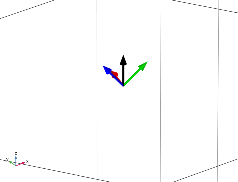
In the Settings window for Arrow Surface, click Replace Expression in the upper-right corner of the Expression section. From the menu, choose Component 1 (comp1) > Electromagnetic Waves, Frequency Domain > Ports > Wave vectors > ewfd.kModex_3,...,ewfd.kModez_3 - Port mode wave vector, port 3.
|
|
3
|
|
4
|
|
1
|
|
2
|
In the Settings window for Arrow Surface, click Replace Expression in the upper-right corner of the Expression section. From the menu, choose Component 1 (comp1) > Electromagnetic Waves, Frequency Domain > Ports > Wave vectors > ewfd.kModex_5,...,ewfd.kModez_5 - Port mode wave vector, port 5.
|
|
3
|
|
4
|
|
1
|
|
2
|
|
3
|
|
4
|
|
5
|
|
1
|
|
2
|
|
3
|
|
4
|
|
5
|
|
6
|
|
1
|
|
2
|
|
3
|
|
4
|
|
5
|
|
6
|
|
7
|
|
8
|
|
9
|
|
10
|
|
11
|
|
12
|
Click OK.
|
|
1
|
|
2
|
Click the Zoom Box button in the Graphics toolbar and then use the mouse to zoom in on the port boundary.
|
|
1
|
|
2
|
|
3
|
|
4
|
|
1
|
|
2
|
|
3
|
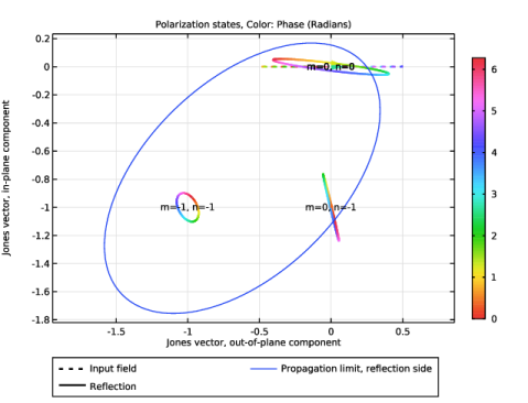
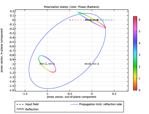
Click Replace Expression in the upper-right corner of the Expression section. From the menu, choose Component 1 (comp1) > Electromagnetic Waves, Frequency Domain > Ports > Polarization state > Jones base vectors > ewfd.eJROOPx_0_0,...,ewfd.eJROOPz_0_0 - Jones base vector on reflection side, out-of-plane direction, order [0,0].
|
|
4
|
|
1
|
|
2
|
|
3
|
Click Replace Expression in the upper-right corner of the Expression section. From the menu, choose Component 1 (comp1) > Electromagnetic Waves, Frequency Domain > Ports > Polarization state > Jones base vectors > ewfd.eJRIPx_0_0,...,ewfd.eJRIPz_0_0 - Jones base vector on reflection side, in-plane direction, order [0,0].
|
|
4
|
|
5
|
|
6
|
Clear the Color checkbox.
|
|
1
|
|
2
|
|
3
|
|
4
|
|
5
|
|
6
|
|
1
|
Right-click Normalized Mode Wave Vector and choose Selection, to only show the wave vector on the port boundary.
|
|
1
|
|
2
|
|
3
|
|
4
|
Click Replace Expression in the upper-right corner of the Expression section. From the menu, choose Component 1 (comp1) > Electromagnetic Waves, Frequency Domain > Geometry and mesh > ewfd.nx,ewfd.ny,ewfd.nz - Normal vector.
|
|
5
|
|
6
|
|
1
|
|
2
|
|
3
|
|
4
|
|
5
|
|
1
|
|
2
|
|
3
|
|
4
|
|
5
|
|
1
|
|
2
|
|
3
|
|
4
|
|
5
|
|
6
|
|
1
|
In the Model Builder window, under Component 1 (comp1) > Electromagnetic Waves, Frequency Domain (ewfd) click Periodic Structure 1.
|
|
2
|
|
4
|
|
1
|
|
1
|
|
2
|
|
1
|
|
2
|
|
3
|
|
4
|
|
1
|
|
2
|
|
3
|
Click
|
|
4
|
|
5
|
|
6
|
Click OK.
|
|
7
|
|
1
|
|
2
|
|
1
|
|
2
|
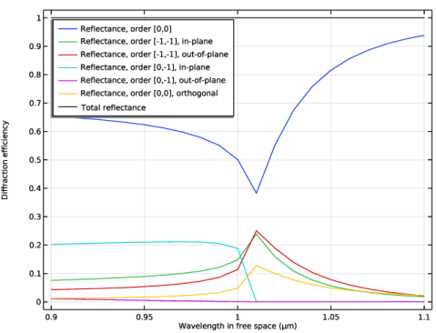
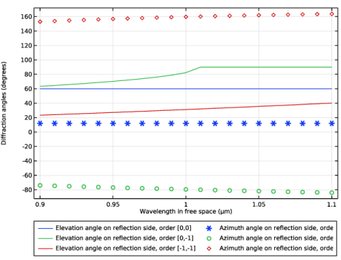
In the Settings window for Global, click Replace Expression in the upper-right corner of the y-Axis Data section. From the menu, choose Component 1 (comp1) > Electromagnetic Waves, Frequency Domain > Ports > Elevation angle, by order > All expressions in this group.
|
|
3
|
|
4
|
|
5
|
|
1
|
|
2
|
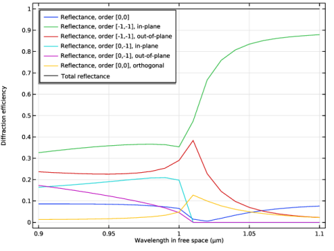
In the Settings window for Global, click Replace Expression in the upper-right corner of the y-Axis Data section. From the menu, choose Component 1 (comp1) > Electromagnetic Waves, Frequency Domain > Ports > Azimuth angle, by order > All expressions in this group.
|
|
3
|
Click to expand the Coloring and Style section. Find the Line style subsection. From the Line list, choose None.
|
|
4
|
|
5
|
|
6
|
|
1
|
|
2
|
|
3
|
|
4
|
Locate the Plot Settings section.
|
|
5
|
|
6
|
|
7
|
|
8
|
|
9
|