|
|
|
 ,
, ,
, .
.
|
1
|
|
2
|
In the Select Physics tree, select Optics > Wave Optics > Electromagnetic Waves, Frequency Domain (ewfd).
|
|
3
|
Click Add.
|
|
4
|
Click
|
|
5
|
|
6
|
Click
|
|
1
|
|
2
|
|
1
|
|
2
|
|
3
|
|
4
|
|
5
|
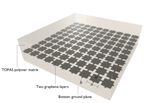
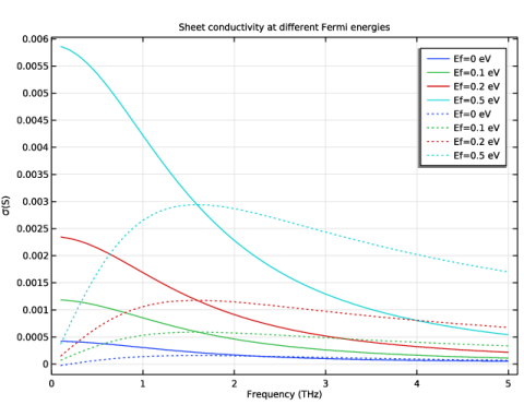
Locate the Definition section. In the Expression text field, type sinh(hbar_const*x/(k_B_const*T))/(cosh(hbar_const*x/(k_B_const*T))+cosh(Ef/(k_B_const*T))).
|
|
6
|
Locate the Units section. In the table, enter the following settings:
|
|
7
|
Locate the Plot Parameters section. In the table, enter the following settings:
|
|
1
|
|
2
|
|
1
|
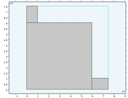
In the Model Builder window, expand the Component 1 (comp1) > Geometry 1 node, then click Geometry 1.
|
|
2
|
|
3
|
|
1
|
|
2
|
|
3
|
|
4
|
|
5
|
|
1
|
|
2
|
|
3
|
|
1
|
|
2
|
|
3
|
|
1
|
|
2
|
|
3
|
|
4
|
|
5
|
|
1
|
|
2
|
|
3
|
|
4
|
|
5
|
|
6
|
|
1
|
In the Model Builder window, under Component 1 (comp1) right-click Materials and choose Blank Material.
|
|
2
|
|
3
|
Locate the Material Contents section. In the table, enter the following settings:
|
|
1
|
|
2
|
|
3
|
Click to expand the Material Properties section. In the Material properties tree, select Basic Properties > Electric Conductivity.
|
|
4
|
Click
|
|
5
|
Locate the Material Contents section. In the table, enter the following settings:
|
|
6
|
Locate the Geometric Entity Selection section. From the Geometric entity level list, choose Boundary.
|
|
7
|
|
1
|
|
1
|
|
1
|
|
3
|
In the Settings window for Transition Boundary Condition, locate the Transition Boundary Condition section.
|
|
4
|
|
5
|
From the εr list, choose User defined. From the μr list, choose User defined. In the d text field, type 2*d_eff.
|
|
1
|
|
2
|
|
3
|
|
1
|
|
2
|
|
3
|
Click
|
|
1
|
|
2
|
|
3
|
|
4
|
|
1
|
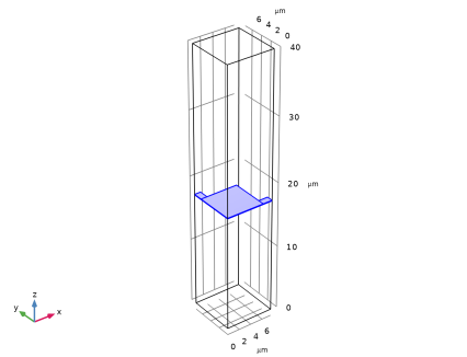
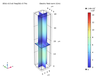
In the Model Builder window, expand the Results > Electric Field (ewfd) node, then click Multislice 1.
|
|
2
|
|
3
|
|
4
|
|
5
|
|
1
|
|
2
|
|
3
|
|
4
|
|
1
|
|
2
|
|
3
|
|
4
|
Locate the Plot Settings section.
|
|
5
|
|
6
|
|
7
|
|
8
|
|
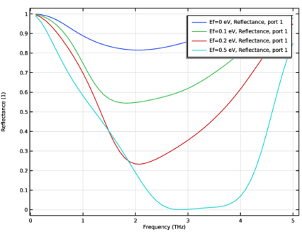
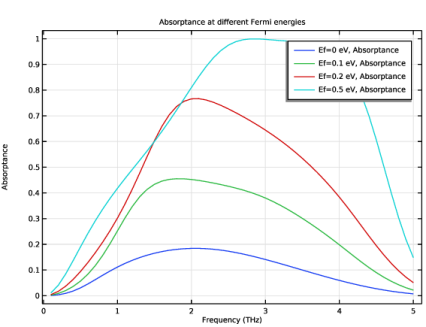
1
|
|
2
|
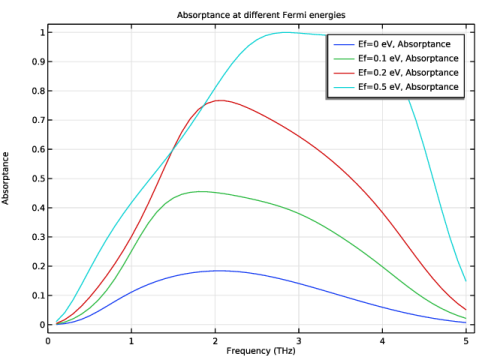
In the Settings window for Global, click Replace Expression in the upper-right corner of the y-Axis Data section. From the menu, choose Component 1 (comp1) > Electromagnetic Waves, Frequency Domain > Heating and losses > ewfd.Atotal - Absorptance - 1.
|
|
3
|
|
1
|
|
2
|
|
3
|
|
4
|
Locate the Plot Settings section.
|
|
5
|
|
6
|
|
7
|
|
8
|
|
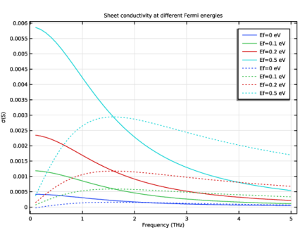
1
|
|
2
|
|
1
|
|
2
|
|
4
|
Click to expand the Coloring and Style section. Find the Line style subsection. From the Line list, choose Dotted.
|
|
5
|
|
6
|