PDF

Enhanced Coating for a Microelectromechanical Mirror
Introduction
Microelectromechanical (MEMS) mirrors are important for spatial light modulators (SLMs), used for instance, in projectors and photolithographic exposure equipment. In order to achieve high efficiency, the mirrors must provide a high reflectance. For lithographic applications, short wavelengths — in the ultraviolet (UV), deep ultraviolet (DUV), or vacuum ultraviolet (VUV) spectral regions — are used to obtain a very high resolution. In addition, as the MEMS mirrors are used in consumer electronics and in industrial processing equipment, the mirrors must survive strong illumination for a long time without degradation.
The most common material for MEMS mirrors is aluminum. However, to make the mirrors more durable and to enhance the reflectance, especially for UV wavelengths, different types of coatings are often applied to the bare MEMS metal mirrors.
This model, adapted from Ref. 1, demonstrates how a coating layer can be applied to a metal mirror to maximize the reflectance at a particular operating wavelength. In this case the MEMS mirror is designed for lithographic applications in the VUV region, at a wavelength of 157 nm.
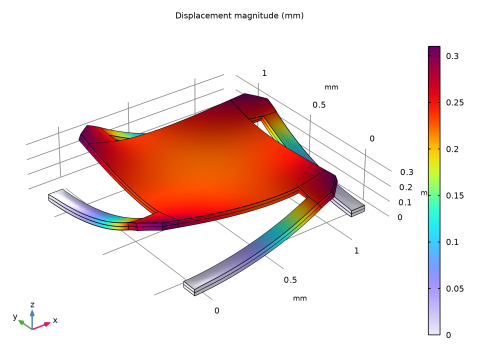
Figure 1: An example of an aluminum MEMS mirror having a reflective center portion, supported by four prestressed plated cantilever springs. This picture is taken from the Prestressed Micromirror model in the MEMS Module Application Library.
Model Definition
The coating layer, lanthanum fluoride (LaF3), and the backing aluminum mirror are modeled using a Layered Impedance Boundary Condition. Thereby neither the coating layer nor the mirror layer need to be modeled using a domain mesh. This can significantly reduce the computation time.
To find the coating thickness that maximizes the reflectance at the operating wavelength, 157 nm, an Optimization study step is used.
Results and Discussion
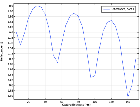
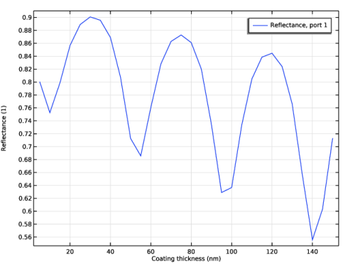
Figure 2 shows the reflectance versus the coating layer thickness. The reflectance has several maxima, but the highest reflectance is obtained for a thickness of about 30 nm. Thus, the optimization procedure consists in finding the maximizing thickness, in the range 10-50 nm.
Figure 2: Reflectance versus coating layer thickness.
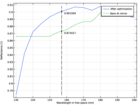
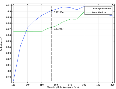
Figure 3 compares the reflectance spectra with only the bare aluminum MEMS mirror and with the combination of the MEMS mirror and the optimized coating layer. At the operating wavelength, the reflectance is larger when the optimal coating layer is applied.
Figure 3: Reflectance spectra for the bare aluminum mirror (denoted Bare Al mirror) and the mirror with the optimized coating layer (denoted After optimization).The optimization procedure allows to achieve a larger reflectance at the 157 nm operation wavelength.
Reference
1. A. Gatto and others, “High-performance coatings for micromechanical mirrors,” Applied Optics, vol. 45, no. 7, pp. 1602–1607, 2006.
Application Library path: Wave_Optics_Module/Couplers_Filters_and_Mirrors/enhanced_mems_mirror_coating
Modeling Instructions
From the File menu, choose New.
New
In the New window, click  Model Wizard.
Model Wizard
1
In the Model Wizard window, click  2D.
2
In the Select Physics tree, select Optics > Wave Optics > Electromagnetic Waves, Frequency Domain (ewfd).
3
Click Add.
4
Click  Study.
5
In the Select Study tree, select Preset Studies for Selected Physics Interfaces > Wavelength Domain.
6
Global Definitions
Parameters 1
1
In the Model Builder window, under Global Definitions click Parameters 1.
2
In the Settings window for Parameters, locate the Parameters section.
3
Geometry 1
Square 1 (sq1)
1
In the Geometry toolbar, click  Square.
2
In the Settings window for Square, locate the Size section.
3
In the Side length text field, type a.
Materials
Air
1
In the Model Builder window, under Component 1 (comp1) right-click Materials and choose Blank Material.
2
In the Settings window for Material, type Air in the Label text field.
3
Locate the Material Contents section. In the table, enter the following settings:
Global Definitions
Now, add the material for the MEMS mirror, which is aluminum.
Add Material
1
In the Materials toolbar, click  Add Material to open the Add Material window.
2
Go to the Add Material window.
3
In the Search text field, type aluminium. Note the British English spelling, which is the one used in the library for the material we want to use.
4
Click Search.
5
In the tree, select Optical > Inorganic Materials > Al - Aluminium and aluminates > Experimental data > Al (Aluminium) (McPeak et al. 2015: n,k 0.15-1.7 um).
6
Right-click and choose Add to Global Materials.
7
In the Materials toolbar, click  Add Material to close the Add Material window.
Materials
Aluminum
1
Right-click Materials and choose More Materials > Material Link.
2
In the Settings window for Material Link, type Aluminum in the Label text field.
3
Locate the Geometric Entity Selection section. From the Geometric entity level list, choose Boundary.
4
Electromagnetic Waves, Frequency Domain (ewfd)
1
In the Model Builder window, under Component 1 (comp1) click Electromagnetic Waves, Frequency Domain (ewfd).
2
In the Settings window for Electromagnetic Waves, Frequency Domain, locate the Components section.
3
From the Electric field components solved for list, choose Out-of-plane vector.
Port 1
1
In the Physics toolbar, click  Boundaries and choose Port.
2
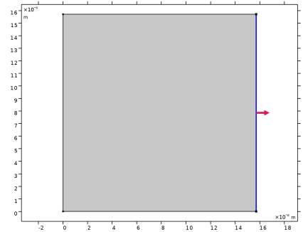
The default Port settings represent a plane wave polarized in the z direction.
Perfect Magnetic Conductor 1
Because the incoming wave is polarized in the z direction, change the top and bottom boundary conditions to Perfect Magnetic Conductor.
1
In the Physics toolbar, click  Boundaries and choose Perfect Magnetic Conductor.
2
Impedance Boundary Condition 1
Initially, use an Impedance boundary condition to represent the MEMS mirror.
1
In the Physics toolbar, click  Boundaries and choose Impedance Boundary Condition.
2
Study 1
Now, compute a reflectance spectrum for the uncoated aluminum MEMS mirror.
Step 1: Wavelength Domain
1
In the Model Builder window, under Study 1 click Step 1: Wavelength Domain.
2
In the Settings window for Wavelength Domain, locate the Study Settings section.
3
From the Wavelength unit list, choose nm.
4
In the Wavelengths text field, type range(130[nm],2[nm],200[nm]).
5
In the Study toolbar, click  Compute.
Results
Reflectance (ewfd)
1
In the Model Builder window, under Results click Reflectance (ewfd).
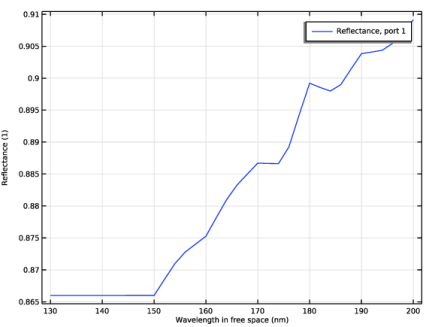
The plot shows that the reflectance decreases the shorter the wavelength is and at 157 nm it is a bit larger than 87%.
Global Definitions
Next, replace the pure aluminum MEMS mirror with a coated mirror. First, add the coating material. Then, replace the Impedance boundary condition with a Layered impedance boundary condition. The Layered impedance boundary condition represents both the aluminum mirror and the coating.
Add Material
1
In the Materials toolbar, click  Add Material to open the Add Material window.
2
Go to the Add Material window.
3
In the Search text field, type Lanthanum.
4
Click Search.
5
In the tree, select Optical > Inorganic Materials > F - Fluorides > Thin film > LaF3 (Lanthanum fluoride) (Rodrìguez-de Marcos et al. 2017: n,k 0.03-2.0 um).
6
Click the Add to Global Materials button in the window toolbar.
7
In the Materials toolbar, click  Add Material to close the Add Material window.
Global Definitions
Layered Material 1 (lmat1)
1
In the Model Builder window, under Global Definitions right-click Materials and choose Layered Material.
2
In the Settings window for Layered Material, locate the Layer Definition section.
3
This layer represents the coating layer, on top of the aluminum mirror.
Materials
Coating Layer
1
In the Model Builder window, under Component 1 (comp1) right-click Materials and choose Layers > Layered Material Link.
2
In the Settings window for Layered Material Link, type Coating Layer in the Label text field.
3
Electromagnetic Waves, Frequency Domain (ewfd)
Layered Impedance Boundary Condition 1
1
In the Physics toolbar, click  Boundaries and choose Layered Impedance Boundary Condition. Notice that the Layered Impedance Boundary Condition can only be added to boundaries where there is a Layered Material. That is why the Layered Material Link was first added to Boundary 4.
2
3
In the Settings window for Layered Impedance Boundary Condition, locate the Substrate Properties section.
4
From the Substrate material list, choose Al (Aluminium) (McPeak et al. 2015: n,k 0.15-1.7 um) (mat2).
Now, the coated mirror is defined, with the Layer Properties taken from the Coating Layer and the Substrate Properties from the mirror material.
Add Study
1
In the Home toolbar, click  Add Study to open the Add Study window.
2
Go to the Add Study window.
3
Find the Studies subsection. In the Select Study tree, select Preset Studies for Selected Physics Interfaces > Wavelength Domain.
4
Click the Add Study button in the window toolbar.
5
In the Home toolbar, click  Add Study to close the Add Study window.
Study 2
Step 1: Wavelength Domain
1
In the Settings window for Wavelength Domain, locate the Study Settings section.
2
In the Wavelengths text field, type lda0.
Make a Parametric Sweep to explore how the reflectance depends on the coating thickness, given a fixed wavelength of 157 nm.
Parametric Sweep
1
In the Study toolbar, click  Parametric Sweep.
2
In the Settings window for Parametric Sweep, locate the Study Settings section.
3
4
5
6
Click  Range.
7
In the Range dialog, type 5[nm] in the Start text field.
8
In the Step text field, type 5[nm].
9
In the Stop text field, type 150[nm].
10
Click Replace.
11
In the Settings window for Parametric Sweep, locate the Study Settings section.
12
13
In the Study toolbar, click  Compute.
Results
Reflectance (ewfd) 1
1
In the Model Builder window, under Results click Reflectance (ewfd) 1.
The plot shows that there are several resonances for different coating thicknesses. However, the highest reflectance is at the first peak, around 30 nm.
Definitions (comp1)
Now, add an Optimization study, to find the coating thickness that gives the maximum reflectance.
Variables 1
1
In the Model Builder window, under Component 1 (comp1) right-click Definitions and choose Variables.
2
In the Settings window for Variables, locate the Variables section.
3
These variables will be used when defining the objective function in the Optimization study.
Add Study
1
In the Home toolbar, click  Add Study to open the Add Study window.
2
Go to the Add Study window.
3
Find the Studies subsection. In the Select Study tree, select Preset Studies for Selected Physics Interfaces > Wavelength Domain.
4
Click the Add Study button in the window toolbar.
5
In the Home toolbar, click  Add Study to close the Add Study window.
Study 3
Step 1: Wavelength Domain
1
In the Settings window for Wavelength Domain, locate the Study Settings section.
2
In the Wavelengths text field, type lda0.
Parameter Optimization
1
In the Study toolbar, click  Optimization and choose Parameter Optimization.
2
In the Settings window for Parameter Optimization, locate the Optimization Solver section.
3
From the Method list, choose Nelder–Mead.
4
Click Add Expression in the upper-right corner of the Objective Function section. From the menu, choose Component 1 (comp1) > Definitions > Variables > comp1.T_Objective - Objective function - 1.
5
Locate the Control Parameters section. Click  Add.
6
7
In the Study toolbar, click  Compute.
Table 1 shows that the optimal coating thickness is 31.03125 nm, with a reflectance of just above 90%.
Root
Finally, compute a new reflectance spectrum using the optimal coating thickness.
Add Study
1
In the Home toolbar, click  Add Study to open the Add Study window.
2
Go to the Add Study window.
3
Find the Studies subsection. In the Select Study tree, select Preset Studies for Selected Physics Interfaces > Wavelength Domain.
4
Click the Add Study button in the window toolbar.
5
In the Home toolbar, click  Add Study to close the Add Study window.
Study 4
Step 1: Wavelength Domain
1
In the Settings window for Wavelength Domain, locate the Study Settings section.
2
From the Wavelength unit list, choose nm.
3
In the Wavelengths text field, type range(130[nm],5[nm],200[nm]).
Parametric Sweep
1
In the Study toolbar, click  Parametric Sweep to specify the optimal coating thickness for this calculation.
2
In the Settings window for Parametric Sweep, locate the Study Settings section.
3
4
5
In the Study toolbar, click  Compute.
Results
Global 1
1
In the Model Builder window, expand the Results > Reflectance (ewfd) node.
2
Right-click Global 1 and choose Copy.
Global 2
1
In the Model Builder window, right-click Reflectance (ewfd) 2 and choose Paste Global.
2
In the Settings window for Global, locate the Data section.
3
From the Dataset list, choose Study 1/Solution 1 (sol1).
4
Click to expand the Legends section. From the Legends list, choose Manual.
5
Graph Marker 1
1
Right-click Global 2 and choose Graph Marker.
2
In the Settings window for Graph Marker, locate the Display section.
3
From the Display mode list, choose Line intersection.
4
In the x-coordinates text field, type 157.
5
Click to expand the Coloring and Style section. From the Anchor point list, choose Upper left.
6
Right-click Graph Marker 1 and choose Copy.
Global 1
1
In the Model Builder window, under Results > Reflectance (ewfd) 2 click Global 1.
2
In the Settings window for Global, locate the Legends section.
3
From the Legends list, choose Manual.
4
Graph Marker 1
1
Right-click Global 1 and choose Paste Graph Marker.
2
In the Settings window for Graph Marker, locate the Display section.
3
Select the Show lines checkbox.
4
Click to expand the Line Style section. From the Line list, choose Dashed.
5
In the Reflectance (ewfd) 2 toolbar, click  Plot.
This plot shows that using a coating layer with optimal thickness results in a larger reflectance, at the operation wavelength of 157 nm.