|
|
|
 ,
,

|
1
|
|
2
|
In the Select Physics tree, select Optics > Wave Optics > Electromagnetic Waves, Frequency Domain (ewfd).
|
|
3
|
Click Add.
|
|
4
|
Click
|
|
5
|
In the Select Study tree, select Preset Studies for Selected Physics Interfaces > Wavelength Domain.
|
|
6
|
Click
|
|
1
|
|
2
|
|
3
|
|
1
|
|
2
|
|
1
|
|
2
|
|
3
|
|
4
|
|
5
|
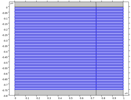
Click to expand the Layers section. In the table, enter the following settings:
|
|
6
|
|
1
|
|
2
|
|
3
|
|
4
|
|
5
|
|
6
|
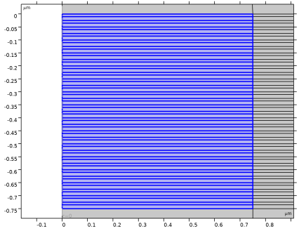
Click to expand the Layers section. In the table, enter the following settings:
|
|
7
|
Clear the Layers on bottom checkbox.
|
|
8
|
Select the Layers to the right checkbox.
|
|
9
|
Click
|
|
10
|
|
1
|
|
2
|
|
3
|
|
4
|
|
5
|
Click
|
|
6
|
|
1
|
|
2
|
|
3
|
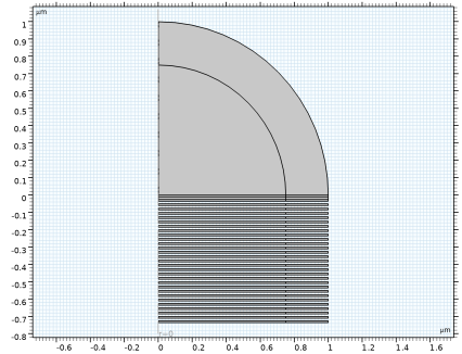
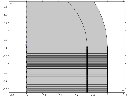
Select the object r1 only.
|
|
4
|
|
5
|
|
6
|
|
7
|
Locate the Selections of Resulting Entities section. Select the Resulting objects selection checkbox.
|
|
8
|
Click
|
|
9
|
|
1
|
|
2
|
|
3
|
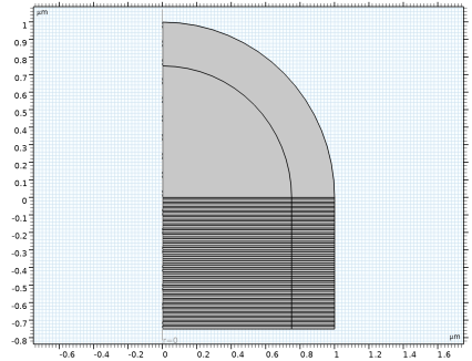
Select the object r2 only.
|
|
4
|
Click
|
|
5
|
|
1
|
|
2
|
|
3
|
|
4
|
|
5
|
|
6
|
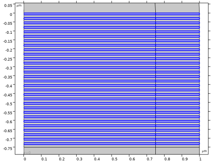
Locate the Layers section. In the table, enter the following settings:
|
|
7
|
Clear the Layers on bottom checkbox.
|
|
8
|
Select the Layers to the right checkbox.
|
|
9
|
Click
|
|
10
|
|
1
|
|
2
|
|
3
|
|
4
|
|
1
|
|
2
|
Go to the Add Material window.
|
|
3
|
|
4
|
Right-click and choose Add to Component 1 (comp1).
|
|
5
|
In the tree, select Optical > Inorganic Materials > Ag - Silver > Experimental data: thin film > Ag (Silver) (Ciesielski et al. 2017: Ag/SiO2; n,k 0.191-20.9 um).
|
|
6
|
Right-click and choose Add to Component 1 (comp1).
|
|
1
|
In the Model Builder window, under Component 1 (comp1) > Materials click Ag (Silver) (Ciesielski et al. 2017: Ag/SiO2; n,k 0.191-20.9 um) (mat2).
|
|
2
|
|
3
|
|
1
|
Go to the Add Material window.
|
|
2
|
In the tree, select Optical > Inorganic Materials > O - Oxygen and oxides > Thin film > SiO2 (Silicon dioxide, Silica, Quartz) (Gao et al. 2013: Thin film; n,k 0.252-1.25 um).
|
|
3
|
Right-click and choose Add to Component 1 (comp1).
|
|
4
|
|
1
|
|
2
|
|
1
|
In the Model Builder window, under Component 1 (comp1) right-click Definitions and choose Variables.
|
|
2
|
|
3
|
Locate the Variables section. In the table, enter the following settings:
|
|
1
|
|
2
|
|
3
|
|
4
|
|
5
|
|
1
|
|
1
|
|
2
|
|
3
|
Click
|
|
4
|
|
5
|
|
6
|
|
7
|
|
8
|
|
9
|
|
1
|
In the Model Builder window, under Component 1 (comp1) click Electromagnetic Waves, Frequency Domain (ewfd).
|
|
2
|
|
3
|
From the Electric field components solved for list, choose In-plane vector, as only the in-plane polarization will be included in the simulation.
|
|
1
|
|
3
|
|
4
|
|
1
|
|
2
|
|
3
|
From the list, choose User-controlled mesh.
|
|
1
|
|
2
|
|
3
|
|
1
|
|
2
|
|
3
|
|
4
|
|
5
|
Click
|
|
1
|
|
2
|
|
3
|
|
4
|
|
1
|
|
2
|
|
3
|
|
4
|
Click
|
|
5
|
|
6
|
|
1
|
|
2
|
|
3
|
|
4
|
|
5
|
|
1
|
|
2
|
|
3
|
|
4
|
|
1
|
|
2
|
|
3
|
|
1
|
|
2
|
|
3
|
|
4
|
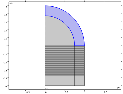
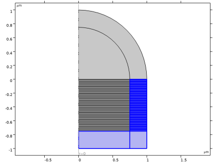
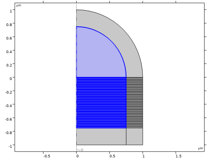
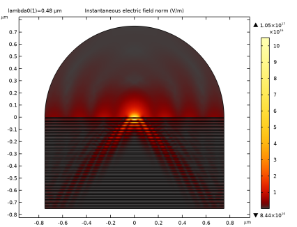
In the Logical expression for inclusion text field, type z<=0. This enables to visualize the fields inside the metamaterial only.
|
|
1
|
|
2
|
|
3
|
|
4
|
|
5
|
|
1
|
|
2
|
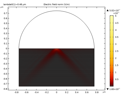
In the Settings window for 2D Plot Group, type Instantaneous Electric Field norm (ewfd) in the Label text field.
|
|
1
|
In the Model Builder window, expand the Instantaneous Electric Field norm (ewfd) node, then click Surface 1.
|
|
2
|
|
3
|
|
1
|
|
2
|
|
3
|
|
1
|
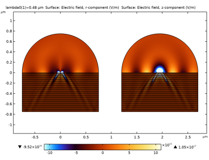
In the Model Builder window, right-click Instantaneous Electric Field norm (ewfd) and choose Duplicate.
|
|
2
|
In the Settings window for 2D Plot Group, type Electric Field Components (ewfd) in the Label text field.
|
|
3
|
|
1
|
In the Model Builder window, expand the Electric Field Components (ewfd) node, then click Surface 1.
|
|
2
|
|
3
|
|
4
|
|
5
|
|
6
|
|
7
|
|
8
|
|
1
|
|
2
|
|
3
|
|
4
|
|
1
|
|
2
|
|
3
|
|
4
|
|
5
|
|
1
|
In the Model Builder window, under Component 1 (comp1) right-click Definitions and choose Variables.
|
|
2
|
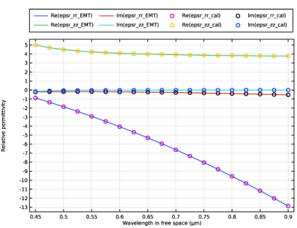
In the Settings window for Variables, type Relative Permittivity, Effective Medium Theory in the Label text field.
|
|
3
|
Locate the Variables section. In the table, enter the following settings:
|
|
1
|
|
2
|
|
3
|
|
4
|
|
5
|
Locate the Variables section. In the table, enter the following settings:
|
|
1
|
|
2
|
|
3
|
Locate the Geometric Entity Selection section. From the Selection list, choose Array 2 - Dielectric Layers.
|
|
4
|
Locate the Variables section. In the table, enter the following settings:
|
|
1
|
|
2
|
In the Settings window for Adjacent, type Metal-dielectric Interior Boundaries in the Label text field.
|
|
3
|
|
4
|
|
5
|
Click OK.
|
|
6
|
|
7
|
|
8
|
|
1
|
|
2
|
|
3
|
|
4
|
|
1
|
|
2
|
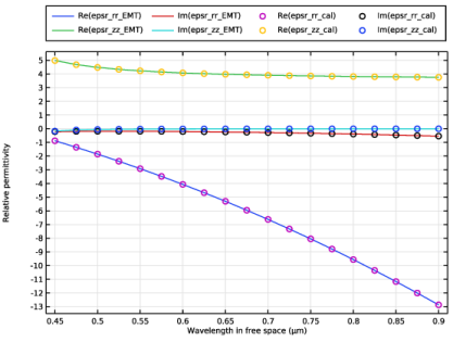
In the Settings window for Variables, type Calculated Effective Relative Permittivity in the Label text field.
|
|
3
|
Locate the Variables section. In the table, enter the following settings:
|
|
1
|
|
2
|
Go to the Add Study window.
|
|
3
|
Find the Studies subsection. In the Select Study tree, select Preset Studies for Selected Physics Interfaces > Wavelength Domain.
|
|
4
|
Right-click and choose Add Study.
|
|
5
|
|
1
|
|
2
|
|
3
|
|
4
|
|
5
|
Clear the Generate default plots checkbox.
|
|
6
|
|
1
|
|
2
|
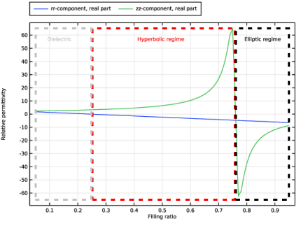
In the Settings window for 1D Plot Group, type Effective Relative Permittivity in the Label text field.
|
|
3
|
|
1
|
|
2
|
|
4
|
|
5
|
|
6
|
|
1
|
|
2
|
|
4
|
Click to expand the Coloring and Style section. Find the Line style subsection. From the Line list, choose None.
|
|
5
|
|
6
|
Locate the Legends section. In the table, enter the following settings:
|
|
1
|
|
2
|
|
3
|
|
4
|
Locate the Plot Settings section.
|
|
5
|
|
6
|
|
7
|
|
8
|
|
9
|