PDF

Band-Gap Analysis of a Photonic Crystal
This application performs a band-gap analysis of a photonic crystal similar to the one used in the Photonic Crystal model.
Introduction
The model investigates the wave propagation in a photonic crystal that consists of GaAs pillars placed equidistant from each other. The distance between the pillars determines a relationship between the wave number and the frequency of the light that prevents light of certain wavelengths from propagating inside the crystal structure. This frequency range is called the photonic band gap (Ref. 2). There are several band gaps for a certain structure, and this application extracts the band gaps for the lowest bands of the crystal.
Model Definition
This model is similar to the Photonic Crystal waveguide model. The difference is that in this model the crystal itself is analyzed instead of a waveguide. Because it has a repeated pattern it is possible to use periodic boundary conditions. As a result, only one pillar is needed for this simulation.
There are two main complications with this band-gap analysis. Firstly, the refractive index of GaAs is frequency dependent, creating a nonlinear eigenfrequency problem. Secondly, the wave vector must be ramped for the band diagram. The first complication can be handled with the use of a nonlinear eigenfrequency solver. The second complication is addressed by adding a parametric sweep to the solver to ramp over the relevant values of the wave vector, k. Furthermore, mode following can be used to automatically group the found eigenfrequencies into the correct bands.
The wave vector for the propagating wave, k, enters the simulation as Floquet periodicity boundary conditions (Ref. 1),
where β is a phase factor determined by the wave vector and the distance, d, between the periodic boundaries:
The range for the swept k is determined by the reciprocal lattice vectors of the photonic crystal, and these are determined from the primitive lattice vectors. For a 2D crystal, there are two lattice vectors, a1 and a2, defined in Figure 1.
Figure 1: Definition of the square primitive cells and the lattice vectors a1 and a2.
The reciprocal lattice vectors are calculated from a1 and a2 using the relations
where a3 is assumed to be the unit vector ez. When a1 and a2 are perpendicular to each other and to a3, b1 and b2 become
Results and Discussion
Figure 2 shows the z-component of the electric field for k = 0.
Figure 2: z-component of the electric field for k = 0.
Figure 3 shows the z-component of the electric field for k = 0.5 for the fifth band.
Figure 3: z-component of the electric field for the fifth band and k = 0.5.
Finally, Figure 4 shows the band diagram for k swept from 0 to 0.5 in the (1,1) direction. Notice that bands two and three are degenerate for k = 0, also that bands one and two along with four and five are degenerate at k = 0.5.
Between bands three and four, there is a frequency range for which there are no states. This frequency range corresponds to a band gap in the structure, as there can be no propagating waves in the (1,1)-propagation direction for that frequency range.
Notice that there is actually a band with a lower frequency than the lowest band in Figure 4. However, the frequencies in this band are so small that the approximation for the frequency-dependent refractive index of GaAs is no longer valid. Thus, this band has not been included in the calculations.
Figure 4: The dispersion relation (frequency versus wave number), when the wave vector is varied in the direction (1,1), for five bands.
References
1. C. Kittel, Introduction to Solid State Physics, 7th ed., John Wiley & Sons, New York, 1996.
2. J.D. Joannopoulos, R.D. Meade, and J.N. Winn, Photonic Crystals (Modeling the Flow of Light), Princeton University Press, 1995.
Application Library path: Wave_Optics_Module/Gratings_and_Metamaterials/bandgap_photonic_crystal
Modeling Instructions
From the File menu, choose New.
New
In the New window, click  Model Wizard.
Model Wizard
1
In the Model Wizard window, click  2D.
2
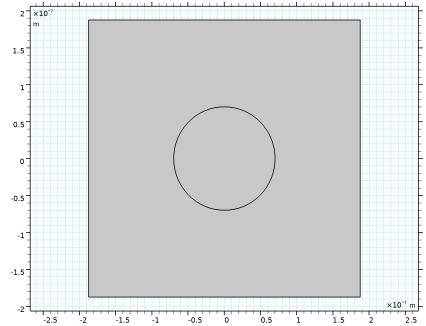
In the Select Physics tree, select Optics > Wave Optics > Electromagnetic Waves, Frequency Domain (ewfd).
3
Click Add.
4
Click  Study.
5
In the Select Study tree, select General Studies > Eigenfrequency.
6
Global Definitions
Parameters 1
First add parameters, characterizing the geometry of the periodic cell.
1
In the Model Builder window, under Global Definitions click Parameters 1.
2
In the Settings window for Parameters, locate the Parameters section.
3
The last parameter, band, will be used for selecting what band to calculate the dispersion relation for.
Definitions
Variables 1
1
In the Model Builder window, under Component 1 (comp1) right-click Definitions and choose Variables.
Add variables representing the reciprocal lattice vector and the Floquet wave vector (used later in the periodic boundary condition).
2
In the Settings window for Variables, locate the Variables section.
3
Geometry 1
The geometry consists of a square air cell surrounding a circular GaAs pillar.
Square 1 (sq1)
1
In the Geometry toolbar, click  Square.
2
In the Settings window for Square, locate the Size section.
3
In the Side length text field, type a.
4
Locate the Position section. From the Base list, choose Center.
Circle 1 (c1)
1
In the Geometry toolbar, click  Circle.
2
In the Settings window for Circle, locate the Size and Shape section.
3
In the Radius text field, type b.
4
Click  Build All Objects.
5
Click the  Zoom Extents button in the Graphics toolbar.
Add Material
1
In the Materials toolbar, click  Add Material to open the Add Material window.
2
Go to the Add Material window.
Define the air, that will surround the GaAs pillar.
3
In the tree, select Built-in > Air.
4
Click the Add to Component button in the window toolbar.
5
In the Materials toolbar, click  Add Material to close the Add Material window.
Definitions
Analytic 1 (an1)
1
In the Definitions toolbar, click  Analytic.
The dispersion relation for the refractive index of GaAs will be used in more than one place, so it is best to define it as an analytical function.
2
In the Settings window for Analytic, type n_GaAs in the Function name text field.
3
Locate the Definition section. In the Expression text field, type -3.3285e5[1/m]*c_const/f+3.8359.
4
In the Arguments text field, type f.
5
Locate the Units section. In the table, enter the following settings:
6
In the Function text field, type 1.
Electromagnetic Waves, Frequency Domain (ewfd)
Compute the solution for out-of-plane polarization.
1
In the Model Builder window, under Component 1 (comp1) click Electromagnetic Waves, Frequency Domain (ewfd).
2
In the Settings window for Electromagnetic Waves, Frequency Domain, locate the Components section.
3
From the Electric field components solved for list, choose Out-of-plane vector.
Periodic Condition 1
1
In the Physics toolbar, click  Boundaries and choose Periodic Condition.
Define the periodic boundary conditions, using the Floquet wave vector.
2
Click the  Zoom Extents button in the Graphics toolbar.
3
4
In the Settings window for Periodic Condition, locate the Periodicity Settings section.
5
From the Type of periodicity list, choose Floquet periodicity.
6
Specify the kF vector as
Periodic Condition 2
1
In the Physics toolbar, click  Boundaries and choose Periodic Condition.
2
3
In the Settings window for Periodic Condition, locate the Periodicity Settings section.
4
From the Type of periodicity list, choose Floquet periodicity.
5
Specify the kF vector as
Add a wave equation feature, representing the GaAs pillar.
Wave Equation, Electric 2
1
In the Physics toolbar, click  Domains and choose Wave Equation, Electric.
2
3
In the Settings window for Wave Equation, Electric, locate the Electric Displacement Field section.
4
From the n list, choose User defined. In the associated text field, type n_GaAs(freq).
5
From the k list, choose User defined. To set the imaginary part of the refractive index to the default value of 0.
Mesh 1
1
In the Model Builder window, under Component 1 (comp1) click Mesh 1.
2
In the Settings window for Mesh, locate the Physics-Controlled Mesh section.
3
From the Element size list, choose Finer.
Define the mesh so that the meshes on opposite edges are identical. This is important for the periodic boundary conditions, so that the source and destination meshes are the same.
Edge 1
1
In the Mesh toolbar, click  More Generators and choose Edge.
2
Copy Edge 1
1
In the Model Builder window, right-click Mesh 1 and choose Copying Operations > Copy Edge.
2
3
In the Settings window for Copy Edge, locate the Destination Boundaries section.
4
Click to select the  Activate Selection toggle button.
5
Copy Edge 2
1
Right-click Mesh 1 and choose Copying Operations > Copy Edge.
2
3
In the Settings window for Copy Edge, locate the Destination Boundaries section.
4
Click to select the  Activate Selection toggle button.
5
Free Triangular 1
1
In the Mesh toolbar, click  Free Triangular.
2
In the Settings window for Free Triangular, click  Build All.
Study 1
Step 1: Eigenfrequency
The ARPACK nonlinear solver is used to handle the nonlinear eigenvalue problem posed by the frequency dependence of the refractive index.
1
In the Model Builder window, under Study 1 click Step 1: Eigenfrequency.
2
In the Settings window for Eigenfrequency, locate the Study Settings section.
3
From the Eigenfrequency solver list, choose ARPACK nonlinear.
4
In the Eigenvalue scaling factor text field, type 1e9.
Find the eigenfrequencies, for k = 0, around 540 THz.
5
Select the Desired number of eigenfrequencies checkbox. In the associated text field, type 5.
6
In the Search for eigenfrequencies around shift text field, type 540[THz].
7
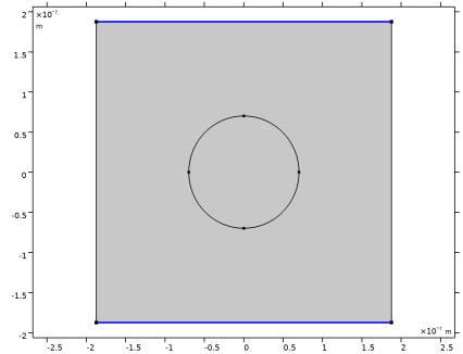
Click to expand the Filtering and Sorting section. Find the Sorting subsection. Select the Mode following checkbox. The Mode following functionality sorts the found eigenfrequencies into the appropriate bands.
Parametric Sweep
1
In the Study toolbar, click  Parametric Sweep.
2
In the Settings window for Parametric Sweep, locate the Study Settings section.
3
4
From the list in the Parameter name column, choose k (Fraction of wave vector magnitude).
5
In the Study toolbar, click  Compute.
Results
Electric Field (ewfd)
1
In the Settings window for 2D Plot Group, locate the Data section.
2
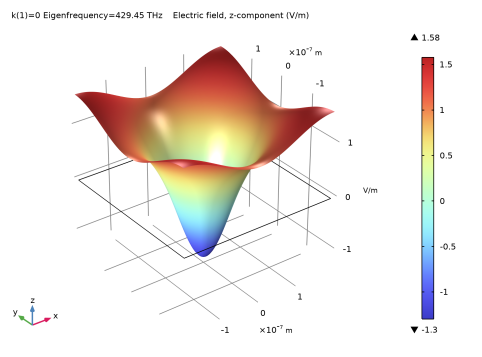
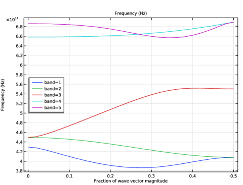
From the Parameter value (k) list, choose 0. To select the results for the center of the Brillouin zone.
3
In the Electric Field (ewfd) toolbar, click  Plot.
Visualize the z component of the electric field, deforming the surface using a height expression.
Surface 1
1
In the Model Builder window, expand the Electric Field (ewfd) node, then click Surface 1.
2
In the Settings window for Surface, locate the Expression section.
3
In the Expression text field, type ewfd.Ez.
Height Expression 1
1
Right-click Surface 1 and choose Height Expression.
2
Click the  Zoom Extents button in the Graphics toolbar. Compare the results with Figure 2.
Electric Field (ewfd)
1
In the Model Builder window, under Results click Electric Field (ewfd).
2
In the Settings window for 2D Plot Group, locate the Data section.
3
From the Parameter value (k) list, choose 0.5.
4
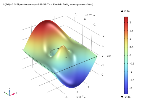
From the Eigenfrequency (THz) list, choose 689.59. To select the result for the Brillouin zone boundary.
5
In the Electric Field (ewfd) toolbar, click  Plot.
6
Click the  Zoom Extents button in the Graphics toolbar. Compare the results with Figure 3.
Band Diagram
1
In the Results toolbar, click  1D Plot Group.
2
In the Settings window for 1D Plot Group, type Band Diagram in the Label text field.
3
Locate the Legend section. From the Position list, choose Middle left.
Global 1
1
Right-click Band Diagram and choose Global.
2
In the Settings window for Global, locate the y-Axis Data section.
3
4
Locate the Data section. From the Dataset list, choose Study 1/Parametric Solutions 1 (sol2).
5
Locate the x-Axis Data section. From the Axis source data list, choose Outer solutions.
6
From the Parameter list, choose Expression.
7
In the Expression text field, type k.
8
Click to expand the Legends section. From the Legends list, choose Manual.
9
10
In the Band Diagram toolbar, click  Plot. Compare the results with Figure 4.