|
|
|
|
1
|
|
2
|
In the Application Libraries window, select Semiconductor Module > Transistors > trench_gate_igbt_2d in the tree.
|
|
3
|
Click
|
|
1
|
|
2
|
|
1
|
|
2
|
|
3
|
|
1
|
|
2
|
|
3
|
Browse to the model’s Application Libraries folder and double-click the file trench_gate_igbt_2d.mph.
|
|
1
|
In the Model Builder window, under Component 2 (comp2) > Geometry 2 > Work Plane 1 (wp1) > Plane Geometry click Point 1 - Emitter contact & doping boundary (pt1).
|
|
2
|
|
3
|
|
4
|
|
1
|
|
2
|
|
1
|
|
2
|
|
3
|
On the object fin, select Boundaries 12, 15, 28, 31, 40, 42, 43, 45, 47, 49, 51, 52, 54, 56, 67, 69, 73, 77, 80, and 82 only.
|
|
4
|
|
5
|
|
6
|
|
7
|
Clear the Automatic detection of small details checkbox.
|
|
1
|
|
2
|
Go to the Add Material window.
|
|
3
|
|
4
|
Click the Add to Component button in the window toolbar.
|
|
5
|
|
1
|
|
2
|
|
1
|
|
2
|
|
1
|
In the Model Builder window, expand the Semiconductor (semi2) node, then click Semiconductor Material Model 1.
|
|
2
|
|
3
|
|
4
|
|
1
|
In the Model Builder window, expand the Semiconductor Material Model 1 node, then click Caughey-Thomas Mobility Model (E) 1.
|
|
2
|
|
3
|
|
4
|
|
1
|
In the Model Builder window, under Component 2 (comp2) > Semiconductor (semi2) click Analytic Doping Model - n-base.
|
|
1
|
|
1
|
|
1
|
|
1
|
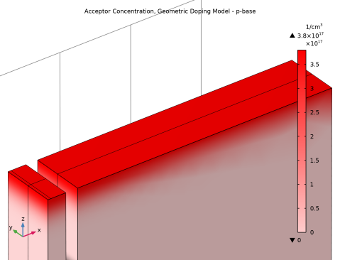
In the Model Builder window, expand the Geometric Doping Model - p-base node, then click Boundary Selection for Doping Profile 1.
|
|
3
|
|
1
|
|
2
|
In the Settings window for Geometric Doping Model, click the Plot Doping Profile for Selected button in the window toolbar.
 |
|
1
|
|
1
|
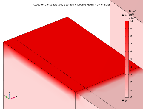
In the Model Builder window, expand the Geometric Doping Model - p+ emitter node, then click Boundary Selection for Doping Profile 1.
|
|
3
|
|
1
|
|
2
|
In the Settings window for Geometric Doping Model, click the Plot Doping Profile for Selected button in the window toolbar.
 |
|
1
|
|
1
|
In the Model Builder window, expand the Geometric Doping Model - n+ emitter node, then click Boundary Selection for Doping Profile 1.
|
|
1
|
In the Model Builder window, under Component 2 (comp2) > Semiconductor (semi2) click Trap-Assisted Recombination 1.
|
|
2
|
|
3
|
|
1
|
|
3
|
|
4
|
|
1
|
|
3
|
|
4
|
|
1
|
|
3
|
|
4
|
|
1
|
|
2
|
|
3
|
|
4
|
|
6
|
Click to expand the Control Entities section. From the Smooth across removed control entities list, choose Off.
|
|
1
|
|
2
|
|
3
|
|
4
|
|
5
|
|
6
|
Select the Reverse direction checkbox.
|
|
1
|
|
2
|
|
3
|
Click the Custom button.
|
|
4
|
|
5
|
|
6
|
|
7
|
|
8
|
|
1
|
|
2
|
|
4
|
Locate the Control Entities section. From the Smooth across removed control entities list, choose Off.
|
|
1
|
|
2
|
|
3
|
|
4
|
|
5
|
|
6
|
Select the Symmetric distribution checkbox.
|
|
1
|
|
3
|
|
4
|
Click to select the
|
|
6
|
Click to expand the Control Entities section. From the Smooth across removed control entities list, choose Off.
|
|
1
|
|
2
|
|
4
|
Click to expand the Control Entities section. From the Smooth across removed control entities list, choose Off.
|
|
5
|
|
1
|
|
3
|
|
4
|
|
5
|
|
6
|
Select the Reverse direction checkbox.
|
|
7
|
|
8
|
|
1
|
|
3
|
|
4
|
Click to select the
|
|
6
|
Locate the Control Entities section. From the Smooth across removed control entities list, choose Off.
|
|
1
|
|
2
|
|
4
|
Locate the Control Entities section. From the Smooth across removed control entities list, choose Off.
|
|
5
|
|
1
|
|
2
|
|
4
|
|
5
|
|
6
|
Select the Reverse direction checkbox.
|
|
1
|
|
2
|
|
4
|
|
5
|
|
1
|
|
2
|
In the Settings window for Distribution, type Distribution 3 - Left surface in the Label text field.
|
|
4
|
|
5
|
|
6
|
|
7
|
Select the Symmetric distribution checkbox.
|
|
1
|
|
2
|
In the Settings window for Distribution, type Distribution 4 - Right surface in the Label text field.
|
|
4
|
|
5
|
|
6
|
|
1
|
|
2
|
In the Settings window for Distribution, type Distribution 5 - Bottom surface in the Label text field.
|
|
4
|
|
5
|
|
6
|
|
7
|
|
1
|
|
3
|
|
4
|
|
5
|
|
1
|
|
3
|
|
4
|
Click to select the
|
|
6
|
Locate the Control Entities section. From the Smooth across removed control entities list, choose Off.
|
|
1
|
|
3
|
|
4
|
|
5
|
|
1
|
|
2
|
|
4
|
|
5
|
|
6
|
|
7
|
Select the Symmetric distribution checkbox.
|
|
1
|
|
2
|
|
4
|
|
5
|
|
1
|
|
2
|
In the Settings window for Distribution, type Distribution 3 - p+ collector in the Label text field.
|
|
4
|
|
5
|
|
6
|
|
7
|
Select the Reverse direction checkbox.
|
|
1
|
|
2
|
|
3
|
|
5
|
Click to expand the Control Entities section. From the Smooth across removed control entities list, choose Off.
|
|
1
|
|
2
|
|
3
|
|
4
|
|
5
|
|
6
|
Select the Reverse direction checkbox.
|
|
1
|
In the Model Builder window, under Component 2 (comp2) > Mesh 2 right-click Swept 1 and choose Duplicate.
|
|
2
|
|
3
|
Click
|
|
1
|
|
2
|
|
3
|
Clear the Reverse direction checkbox.
|
|
4
|
|
5
|
|
1
|
|
2
|
|
1
|
In the Model Builder window, expand the Study 1 - 2D node, then click Step 1: Semiconductor Equilibrium.
|
|
2
|
In the Settings window for Semiconductor Equilibrium, locate the Physics and Variables Selection section.
|
|
3
|
Select the Modify model configuration for study step checkbox.
|
|
4
|
|
5
|
Click
|
|
1
|
|
2
|
|
3
|
Select the Modify model configuration for study step checkbox.
|
|
4
|
|
5
|
Click
|
|
1
|
|
2
|
Go to the Add Study window.
|
|
3
|
|
4
|
Click the Add Study button in the window toolbar.
|
|
5
|
|
1
|
In the Model Builder window, under Study 1 - 2D, Ctrl-click to select Step 1: Semiconductor Equilibrium and Step 2: Stationary.
|
|
2
|
Right-click and choose Copy.
|
|
1
|
In the Settings window for Semiconductor Equilibrium, locate the Physics and Variables Selection section.
|
|
2
|
|
3
|
Click
|
|
4
|
|
5
|
Click
|
|
1
|
|
2
|
|
3
|
|
4
|
Click
|
|
5
|
|
6
|
Click
|
|
7
|
|
1
|
In the Model Builder window, expand the Study 2 - 3D > Solver Configurations > Solution 3 (sol3) node, then click Dependent Variables 2.
|
|
2
|
|
3
|
|
4
|
In the Model Builder window, expand the Study 2 - 3D > Solver Configurations > Solution 3 (sol3) > Dependent Variables 2 node, then click Voltage Drop Across Contact (comp2.semi2.V_dae).
|
|
5
|
|
6
|
|
7
|
|
1
|
|
2
|
|
3
|
|
4
|
|
5
|
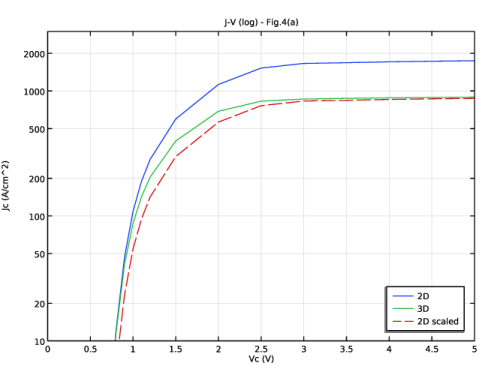
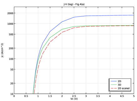
Locate the y-Axis Data section. In the table, enter the following settings:
|
|
1
|
|
2
|
|
3
|
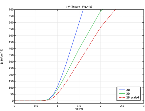
Locate the y-Axis Data section. In the table, enter the following settings:
|
|
4
|
Click to expand the Coloring and Style section. Find the Line style subsection. From the Line list, choose Dashed.
|
|
1
|
|
2
|
|
3
|
|
4
|
Locate the Plot Settings section.
|
|
5
|
|
6
|
|
1
|
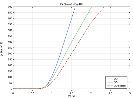
In the Model Builder window, under Results > J-V (log) - Fig.4(a), Ctrl-click to select Global 1 - 3D and Global 1 - 2D scaled.
|
|
2
|
Right-click and choose Copy.
|
|
1
|
In the Model Builder window, under Results right-click J-V (linear) - Fig.4(b) and choose Paste Multiple Items.
|
|
2
|
|
3
|
|
4
|
Locate the Plot Settings section.
|
|
5
|
|
6
|
|
1
|
In the Model Builder window, under Component 2 (comp2) > Semiconductor (semi2) click Thin Insulator Gate 1.
|
|
2
|
|
3
|
Click
|
|
1
|
|
2
|
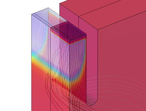
In the Settings window for 3D Plot Group, type Electron Concentration & Current Streamlines 3D in the Label text field.
|
|
1
|
|
2
|
In the Settings window for Streamline, type Streamline 1 - Electron current in the Label text field.
|
|
3
|
Click Replace Expression in the upper-right corner of the Expression section. From the menu, choose Component 2 (comp2) > Semiconductor > Currents and charge > Electron current > semi2.JnX,...,semi2.JnZ - Electron current density.
|
|
5
|
Locate the Coloring and Style section. Find the Point style subsection. From the Color list, choose Black.
|
|
1
|
|
2
|
|
3
|
Click Replace Expression in the upper-right corner of the Expression section. From the menu, choose Component 2 (comp2) > Semiconductor > Currents and charge > Hole current > semi2.JpX,...,semi2.JpZ - Hole current density.
|
|
5
|
Locate the Coloring and Style section. Find the Point style subsection. From the Color list, choose White.
|
|
1
|
|
2
|
|
3
|