
|
|
|
|
1
|
|
2
|
|
3
|
Click Add.
|
|
4
|
Click
|
|
5
|
In the Select Study tree, select Preset Studies for Selected Physics Interfaces > Semiconductor Equilibrium.
|
|
6
|
Click
|
|
1
|
|
2
|
|
3
|
|
4
|
Locate the Parameters section. In the table, enter the following settings:
|
|
1
|
|
2
|
|
3
|
|
1
|
|
2
|
|
3
|
|
4
|
|
5
|
|
6
|
Click to expand the Layers section. In the table, enter the following settings:
|
|
7
|
Clear the Layers on bottom checkbox.
|
|
8
|
Select the Layers on top checkbox.
|
|
1
|
|
2
|
|
3
|
|
4
|
|
5
|
|
6
|
|
1
|
|
2
|
|
3
|
|
4
|
|
5
|
|
6
|
|
7
|
|
1
|
|
2
|
|
3
|
|
4
|
|
5
|
|
6
|
|
7
|
|
1
|
|
2
|
|
3
|
|
4
|
|
5
|
|
6
|
|
7
|
Locate the Layers section. In the table, enter the following settings:
|
|
8
|
Select the Layers to the left checkbox.
|
|
9
|
Clear the Layers on bottom checkbox.
|
|
1
|
|
2
|
On the object r3, select Points 1 and 2 only.
|
|
3
|
On the object r4, select Point 1 only.
|
|
4
|
|
5
|
|
1
|
|
2
|
|
3
|
|
4
|
|
5
|
|
1
|
|
2
|
|
3
|
|
1
|
|
2
|
|
3
|
|
4
|
|
5
|
|
6
|
|
1
|
|
2
|
|
3
|
|
4
|
|
5
|
|
6
|
|
1
|
|
2
|
|
3
|
|
4
|
|
5
|
|
6
|
|
1
|
|
2
|
|
3
|
|
4
|
|
5
|
|
6
|
|
7
|
Click
|
|
1
|
|
2
|
In the Settings window for Explicit Selection, type All domains before oxide in the Label text field.
|
|
3
|
|
4
|
Select the object dif1 only.
|
|
5
|
|
1
|
|
2
|
In the Settings window for Adjacent Selection, type All exterior boundaries before oxide in the Label text field.
|
|
3
|
|
4
|
|
5
|
Click OK.
|
|
1
|
|
2
|
|
3
|
|
4
|
|
5
|
|
6
|
|
7
|
|
1
|
|
2
|
In the Settings window for Intersection Selection, type Top boundaries for oxide in the Label text field.
|
|
3
|
|
4
|
|
5
|
|
6
|
Click OK.
|
|
7
|
|
8
|
Click
|
|
9
|
|
10
|
Click OK.
|
|
11
|
|
12
|
|
1
|
|
2
|
|
3
|
|
4
|
|
5
|
|
1
|
|
2
|
Select the object dif1 only.
|
|
3
|
|
4
|
|
5
|
Select the object pt1 only.
|
|
6
|
|
1
|
|
2
|
On the object off1, select Point 1 only.
|
|
3
|
|
4
|
|
5
|
On the object dif1, select Point 7 only.
|
|
1
|
|
2
|
On the object pt1, select Point 1 only.
|
|
3
|
|
4
|
|
5
|
On the object mov1, select Point 1 only.
|
|
1
|
|
2
|
On the object off1, select Point 17 only.
|
|
3
|
|
4
|
|
5
|
On the object dif1, select Point 29 only.
|
|
1
|
|
2
|
On the object off1, select Point 18 only.
|
|
3
|
|
4
|
|
5
|
On the object dif1, select Point 34 only.
|
|
1
|
|
2
|
On the object off1, select Point 27 only.
|
|
3
|
|
4
|
|
5
|
On the object dif1, select Point 46 only.
|
|
1
|
In the Model Builder window, under Component 1 (comp1) > Geometry 1, Ctrl-click to select Line Segment 1 (ls1), Line Segment 2 (ls2), Line Segment 3 (ls3), Line Segment 4 (ls4), and Line Segment 5 (ls5).
|
|
2
|
Right-click and choose Group.
|
|
1
|
|
2
|
|
1
|
|
2
|
|
3
|
|
4
|
On the object csol1, select Domains 7 and 20 only.
|
|
1
|
|
2
|
On the object del1, select Points 9, 47, and 53 only.
|
|
3
|
|
4
|
|
1
|
|
2
|
|
3
|
|
4
|
Select the object cha1 only.
|
|
5
|
|
1
|
|
2
|
In the Settings window for Adjacent Selection, type All exterior boundaries in the Label text field.
|
|
3
|
|
4
|
|
5
|
Click OK.
|
|
6
|
|
7
|
|
1
|
|
2
|
|
3
|
|
4
|
|
5
|
|
6
|
|
7
|
|
1
|
|
2
|
|
3
|
|
4
|
|
5
|
|
6
|
Click OK.
|
|
7
|
|
8
|
Click
|
|
9
|
|
10
|
Click OK.
|
|
1
|
|
2
|
|
3
|
|
4
|
|
5
|
|
6
|
|
7
|
|
8
|
|
9
|
|
1
|
|
2
|
In the Settings window for Intersection Selection, type Field contact for ring 1 in the Label text field.
|
|
3
|
|
4
|
|
5
|
|
6
|
Click OK.
|
|
7
|
|
8
|
Click
|
|
9
|
|
10
|
Click OK.
|
|
1
|
|
2
|
Go to the Add Material window.
|
|
3
|
In the tree, select Semiconductors > SiC - Silicon Carbide > SiC - Silicon Carbide [solid,4H Polytype].
|
|
4
|
Click the Add to Component button in the window toolbar.
|
|
5
|
|
6
|
Click the Add to Component button in the window toolbar.
|
|
7
|
|
1
|
|
2
|
|
3
|
Click OK.
|
|
4
|
|
5
|
|
6
|
|
1
|
In the Model Builder window, under Component 1 (comp1) > Semiconductor (semi) click Semiconductor Material Model 1.
|
|
2
|
|
3
|
|
4
|
|
1
|
|
2
|
|
3
|
|
4
|
Find the Expression for remaining selection subsection. In the Temperature text field, type T_lattice.
|
|
1
|
In the Model Builder window, under Component 1 (comp1) > Semiconductor (semi) click Semiconductor Material Model 1.
|
|
2
|
In the Settings window for Semiconductor Material Model, click to expand the Dopant Ionization section.
|
|
3
|
|
4
|
|
5
|
|
1
|
|
3
|
|
4
|
|
1
|
|
2
|
|
3
|
|
1
|
|
2
|
|
3
|
|
1
|
In the Model Builder window, under Component 1 (comp1) > Semiconductor (semi), Ctrl-click to select Impact Ionization Generation 1 and Trap-Assisted Recombination 1.
|
|
2
|
Right-click and choose Group.
|
|
1
|
|
2
|
In the Settings window for Analytic Doping Model, type P-type contact doping in the Label text field.
|
|
4
|
|
1
|
|
2
|
|
4
|
|
1
|
|
2
|
|
4
|
|
5
|
|
1
|
|
2
|
|
4
|
|
5
|
|
1
|
In the Model Builder window, under Component 1 (comp1) > Semiconductor (semi), Ctrl-click to select P-type contact doping, P-type anode doping, N-type drift region, and N-type substrate.
|
|
2
|
Right-click and choose Group.
|
|
1
|
|
2
|
|
3
|
|
4
|
In the list box, select 31 (not applicable).
|
|
5
|
|
6
|
|
1
|
|
2
|
|
3
|
|
4
|
|
1
|
|
2
|
|
4
|
|
1
|
|
2
|
|
3
|
|
4
|
|
1
|
|
2
|
|
3
|
|
4
|
|
5
|
|
1
|
In the Model Builder window, under Component 1 (comp1) > Mesh 1 right-click Size 1 and choose Duplicate.
|
|
2
|
|
4
|
|
5
|
|
6
|
Click
|
|
1
|
|
2
|
|
1
|
|
2
|
|
3
|
Select the Auxiliary sweep checkbox.
|
|
4
|
Click
|
|
1
|
|
2
|
Expand the Solution 1 (sol1) node.
|
|
3
|
|
4
|
|
5
|
|
6
|
|
7
|
|
8
|
|
9
|
|
10
|
|
11
|
|
12
|
|
13
|
|
14
|
|
15
|
|
16
|
|
17
|
|
18
|
In the Model Builder window, expand the High-Temperature Reverse Sweep > Solver Configurations > Solution 1 (sol1) > Stationary Solver 2 node, then click Parametric 1.
|
|
19
|
|
20
|
Select the Tuning of step size checkbox.
|
|
21
|
|
22
|
|
23
|
|
24
|
|
25
|
|
26
|
|
28
|
|
29
|
Clear the Add information checkbox.
|
|
30
|
|
1
|
|
2
|
|
1
|
|
2
|
|
4
|
|
5
|
|
6
|
|
1
|
|
2
|
|
1
|
|
2
|
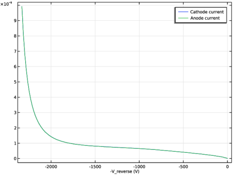
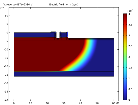
In the Settings window for Surface, click Replace Expression in the upper-right corner of the Expression section. From the menu, choose Component 1 (comp1) > Semiconductor > Electric > semi.normE - Electric field norm - V/m.
|
|
3
|
|
4
|
Click
|
|
5
|
|
6
|
|
7
|
Click
|
|
1
|
|
2
|
|
1
|
|
2
|
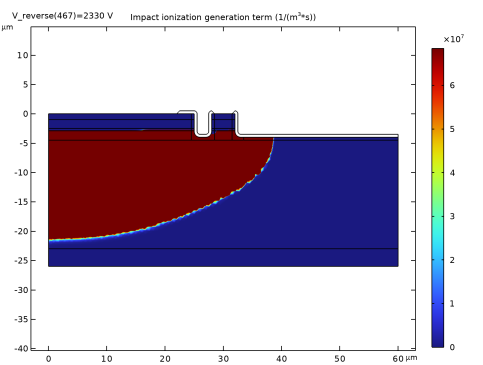
In the Settings window for Surface, click Replace Expression in the upper-right corner of the Expression section. From the menu, choose Component 1 (comp1) > Semiconductor > Generation and recombination > semi.Gii - Impact ionization generation term - 1/(m³·s).
|
|
3
|
|
4
|
|
5
|
|
6
|