PDF

Reverse Bias Leakage Current
Introduction
In a diode or a transistor, upon a reverse-biased p–n junction, ideally no current should flow. However, due to presence of minority carriers (electrons on the p-side and holes on the n-side), a small current, known as the reverse-bias leakage current, does flow. While the reverse-bias leakage current is typically small, it plays a crucial role in the overall behavior and performance of semiconductor devices. Managing and minimizing this current is essential for optimizing power efficiency and precision for various applications.
This example shows how a mixed formulation is beneficial for calculating the small leakage current accurately.
Model Definition
Figure 1 shows the 1D model of a PIN diode together with the net doping concentration along the device. The diode consists of three domains, each 1 μm in length. The doping levels corresponding to each domain are defined using the Analytic Doping Model feature and the electrodes are defined on both ends using the Metal Contact feature. In order to compare the accuracy of the mixed formulation in calculating small leakage currents, two studies are performed. First, with the finite-element quasi-Fermi level discretization, and second, with mixed finite-element log formulation.
Figure 1: Net doping concentration along the PIN diode, where the 1D modeled device is shown at the bottom.
The procedure of the implementation is described in detail in the Modeling Instructions section.
Results and Discussion
Figure 2 shows the comparison of electron and hole current densities calculated with different discretizations, namely the FEM and mixed formulations.
Figure 2: Comparison between current densities calculated with FEM versus Mixed Formulation.
Application Library path: Semiconductor_Module/Photonic_Devices_and_Sensors/reverse_bias_leakage_current
Modeling Instructions
From the File menu, choose New.
New
In the New window, click  Model Wizard.
Model Wizard
1
In the Model Wizard window, click  1D.
2
In the Select Physics tree, select Semiconductor > Semiconductor (semi).
3
Click Add.
4
Click Add.
5
Click  Study.
6
In the Select Study tree, select General Studies > Stationary.
7
Global Definitions
Parameters 1
1
In the Model Builder window, under Global Definitions click Parameters 1.
2
In the Settings window for Parameters, locate the Parameters section.
3
Geometry 1
1
In the Model Builder window, under Component 1 (comp1) click Geometry 1.
2
In the Settings window for Geometry, locate the Units section.
3
From the Length unit list, choose µm.
Interval 1 (i1)
1
Right-click Component 1 (comp1) > Geometry 1 and choose Interval.
2
In the Settings window for Interval, locate the Interval section.
3
From the Coordinate source list, choose Vector.
4
In the Coordinates text field, type 0,1,2,3.
Add Material
1
In the Materials toolbar, click  Add Material to open the Add Material window.
2
Go to the Add Material window.
3
In the tree, select Semiconductors > Si - Silicon.
4
Click the Add to Component button in the window toolbar.
5
In the Materials toolbar, click  Add Material to close the Add Material window.
Semiconductor (semi)
1
In the Settings window for Semiconductor, click to expand the Discretization section.
2
From the Formulation list, choose Finite element quasi Fermi level (quadratic shape function).
Analytic Doping Model 1
1
In the Physics toolbar, click  Domains and choose Analytic Doping Model.
2
3
In the Settings window for Analytic Doping Model, locate the Impurity section.
4
From the Impurity type list, choose Donor doping (n-type).
5
In the ND0 text field, type Ndop.
Analytic Doping Model 2
1
Right-click Analytic Doping Model 1 and choose Duplicate.
2
3
In the Settings window for Analytic Doping Model, locate the Impurity section.
4
From the Impurity type list, choose Acceptor doping (p-type).
5
In the NA0 text field, type 1e14[1/cm^3].
Analytic Doping Model 3
1
Right-click Analytic Doping Model 2 and choose Duplicate.
2
3
In the Settings window for Analytic Doping Model, locate the Impurity section.
4
In the NA0 text field, type Ndop.
Metal Contact 1
1
In the Physics toolbar, click  Boundaries and choose Metal Contact.
2
Metal Contact 2
1
Right-click Metal Contact 1 and choose Duplicate.
2
3
In the Settings window for Metal Contact, locate the Terminal section.
4
In the V0 text field, type Va.
5
Semiconductor 2 (semi2)
1
In the Model Builder window, under Component 1 (comp1) click Semiconductor 2 (semi2).
2
In the Settings window for Semiconductor, locate the Discretization section.
3
From the Formulation list, choose Mixed finite element, log formulation (linear shape function).
Semiconductor (semi)
Analytic Doping Model 1, Analytic Doping Model 2, Analytic Doping Model 3
1
In the Model Builder window, under Component 1 (comp1) > Semiconductor (semi), Ctrl-click to select Analytic Doping Model 1, Analytic Doping Model 2, and Analytic Doping Model 3.
2
Semiconductor 2 (semi2)
Analytic Doping Model 4
Drag and drop on Semiconductor 2 (semi2).
Semiconductor (semi)
Metal Contact 1, Metal Contact 2
1
In the Model Builder window, under Component 1 (comp1) > Semiconductor (semi), Ctrl-click to select Metal Contact 1 and Metal Contact 2.
2
Semiconductor 2 (semi2)
Metal Contact 3
Drag and drop on Semiconductor 2 (semi2).
Study 1
Step 1: Stationary
1
In the Model Builder window, under Study 1 click Step 1: Stationary.
2
In the Settings window for Stationary, locate the Study Settings section.
3
From the Tolerance list, choose User controlled.
4
Locate the Physics and Variables Selection section. In the Solve for column of the table, under Component 1 (comp1), clear the checkbox for Semiconductor 2 (semi2).
5
Locate the Study Settings section. In the Relative tolerance text field, type 1.0E-4.
6
In the Model Builder window, click Study 1.
7
In the Settings window for Study, locate the Study Settings section.
8
Clear the Generate default plots checkbox.
9
In the Study toolbar, click  Compute.
Add Study
1
In the Study toolbar, click  Add Study to open the Add Study window.
2
Go to the Add Study window.
3
Find the Studies subsection. In the Select Study tree, select General Studies > Stationary.
4
Click the Add Study button in the window toolbar.
Study 2
1
In the Settings window for Stationary, locate the Study Settings section.
2
From the Tolerance list, choose User controlled.
3
Locate the Physics and Variables Selection section. In the Solve for column of the table, under Component 1 (comp1), clear the checkbox for Semiconductor (semi).
4
Locate the Study Settings section. In the Relative tolerance text field, type 1E-4.
5
Click to expand the Study Extensions section. Select the Auxiliary sweep checkbox.
6
7
8
9
10
From the Sweep type list, choose All combinations.
Step 2: Stationary 2
1
In the Study toolbar, click  Stationary.
2
In the Settings window for Stationary, locate the Study Settings section.
3
From the Tolerance list, choose User controlled.
4
In the Relative tolerance text field, type 1E-4.
5
Locate the Physics and Variables Selection section. In the Solve for column of the table, under Component 1 (comp1), clear the checkbox for Semiconductor (semi).
6
Click to expand the Study Extensions section. Select the Auxiliary sweep checkbox.
7
8
9
In the Model Builder window, click Study 2.
10
In the Settings window for Study, locate the Study Settings section.
11
Clear the Generate default plots checkbox.
12
In the Study toolbar, click  Compute.
Results
JnX and JpX Comparison
1
In the Results toolbar, click  1D Plot Group.
2
In the Settings window for 1D Plot Group, click to expand the Title section.
3
From the Title type list, choose Manual.
4
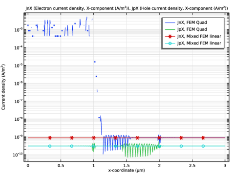
In the Title text area, type JnX (Electron current density, X-component (A/m<sup>2</sup>)), JpX (Hole current density, X-component (A/m<sup>2</sup>)).
5
In the Label text field, type JnX and JpX Comparison.
6
Locate the Plot Settings section.
7
Select the x-axis label checkbox. In the associated text field, type x-coordinate (µm).
8
Select the y-axis label checkbox. In the associated text field, type Current density (A/m<sup>2</sup>).
9
Locate the Axis section. Select the y-axis log scale checkbox.
Line Graph 1
1
Right-click JnX and JpX Comparison and choose Line Graph.
2
In the Settings window for Line Graph, locate the Selection section.
3
From the Selection list, choose All domains.
4
Locate the y-Axis Data section. In the Expression text field, type semi.JnX.
5
Locate the x-Axis Data section. From the Parameter list, choose Expression.
6
In the Expression text field, type x.
7
Click to expand the Legends section. Select the Show legends checkbox.
8
From the Legends list, choose Manual.
9
Line Graph 2
1
Right-click Line Graph 1 and choose Duplicate.
2
In the Settings window for Line Graph, locate the y-Axis Data section.
3
In the Expression text field, type semi.JpX.
4
Locate the Legends section. In the table, enter the following settings:
Line Graph 3
1
Right-click Line Graph 2 and choose Duplicate.
2
In the Settings window for Line Graph, locate the Data section.
3
From the Dataset list, choose Study 2/Solution 2 (sol2).
4
From the Parameter selection (Ndop) list, choose Last.
5
Locate the y-Axis Data section. In the Expression text field, type semi2.JnX.
6
Locate the Legends section. In the table, enter the following settings:
7
Click to expand the Coloring and Style section. Find the Line markers subsection. From the Marker list, choose Cycle.
8
From the Positioning list, choose Interpolated.
Line Graph 4
1
Right-click Line Graph 3 and choose Duplicate.
2
In the Settings window for Line Graph, locate the y-Axis Data section.
3
In the Expression text field, type semi2.JpX.
4
Locate the Legends section. In the table, enter the following settings:
5
In the JnX and JpX Comparison toolbar, click  Plot.