PDF

P–N Junction 1D
This model sets up a simple 1D benchmark of a p–n junction, or semiconductor diode, based on an example given in Ref. 1.
Introduction
A semiconductor diode consists of two regions with different doping: a p-type region with a dominant concentration of holes, and an n-type region with a dominant concentration of electrons. The anode contact is adjacent to the p-type region, and the cathode connects to the n-type region. Impurities that the manufacturing process adds to the semiconductor material determine each region’s doping type. Donor impurities add additional electrons to the material conduction band and create n-type material. Acceptor impurities remove electrons from the valence band and create p-type material.
It is possible to derive a semiconductor model from Maxwell’s equations and the Boltzmann equation for carrier transport. The three basic semiconductor equations (for a stationary problem) are
where ε is the dielectric permittivity of the semiconductor; V is the electric potential; p and n are the electron and hole concentrations, respectively; ND+ and NA- are the concentrations of ionized donors and acceptors, respectively; Jn and Jp are the electron and hole currents, respectively; and RSRH is the Shockley–Read–Hall recombination rate (see below for a description; in this case this term is assumed to be the only source of electron and hole recombination).
The electron and hole currents can be expressed in terms of V, n, and p in the following manner (assuming an isothermal, nondegenerate semiconductor with a constant band structure):
where μn and μp are the carrier mobilities, kB is Boltzmann’s constant, and T is the absolute temperature. In this model, the mobility is a complex-valued function of the temperature and the donor and acceptor concentrations, as defined in Ref. 1.
The term RSRH gives the rate at which electrons recombine (by a mechanism known as Shockley–Read–Hall recombination, which is often dominant in silicon). This recombination process involves traps in the forbidden band gap of the semiconductor. The recombination rate due to this mechanism is given by
where ni is the intrinsic carrier concentration (that is, the carrier concentration in an undoped semiconductor), τn and τp are the carrier lifetimes, and n1 and p1 are parameters related to the trap energy level. If the trap level is located at the middle of the band gap (which is assumed in this model), then n1 and p1 equal ni.
Model Definition
This model simulates the behavior of a p–n junction under reverse, equilibrium, and forward bias. The modeled junction has a length of 5 μm and a net doping concentration of × 1015 cm-3 for both the p- and n-doped side. A Shockley–Read–Hall recombination feature is also added to the model in order to simulate recombination usually observed in indirect band-gap semiconductor such as silicon, which is the material used in this model. The model uses the material parameters used in Ref. 1 and compares the carrier concentration profiles obtained from the computation with those obtained in the reference under different biasing conditions (4 V, 0 V, and 0.5 V). Two different discretization methods are used to solve the model: the Finite Element Log Formation discretization and the Finite Volume discretization. The results of these two computation methods are found to be in good agreement.
Results and Discussion
Figure 1shows the electric potential in the junction for different biasing conditions. A good agreement is shown between the finite element, finite volume, and reference for all biasing conditions. Figure 2, Figure 4, and Figure 6 show the energy diagrams for each biasing conditions. These figures display a perfect agreement between the finite element (using streamline-diffusion stabilization) and finite volume computations. Comparing the carrier concentrations also shows a very good agreement between the reference, finite element, and finite volume computations — see Figure 3, Figure 5, and Figure 7.
Figure 1: Electric potential obtained using the finite element (FE) and finite volume (FV) methods under different bias, that is, reverse (Rev), equilibrium (Eq), and forward (Fwd) bias. The results are compared to those calculated in Ref. 1(Kramer)
Figure 2: Energy diagram obtained using the finite element (FE) and finite volume (FV) methods under reverse bias (-4 V).
Figure 3: Electron and hole concentrations obtained using the finite element (FE) and finite volume (FV) methods under reverse bias (-4 V). The profiles are compared to those calculated in Ref. 1(Kramer).
Figure 4: Energy diagram obtained using the finite element (FE) and finite volume (FV) methods at equilibrium (0 V).
Figure 5: Electron and hole concentrations obtained using the finite element (FE) and finite volume (FV) methods at equilibrium (0 V). The profiles are compared to those calculated in Ref. 1(Kramer).
Figure 6: Energy diagram obtained using the finite element (FE) and finite volume (FV) methods under forward bias (0.5 V).
Figure 7: Electron and hole concentrations obtained using the finite element (FE) and finite volume (FV) methods under forward bias (0.5 V). The profiles are compared to those calculated in Ref. 1(Kramer).
Reference
1. K.M. Kramer and W.N.G. Hitchon, Semiconductor Devices a Simulation Approach, Prentice Hall, Upper Saddle River, NJ, 1997.
Application Library path: Semiconductor_Module/Verification_Examples/pn_junction_1d
Modeling Instructions
From the File menu, choose New.
New
In the New window, click  Model Wizard.
Model Wizard
1
In the Model Wizard window, click  1D.
2
In the Select Physics tree, select Semiconductor > Semiconductor (semi).
3
Click Add.
4
Click  Study.
5
In the Select Study tree, select General Studies > Stationary.
6
Semiconductor (semi)
1
In the Model Builder window, under Component 1 (comp1) click Semiconductor (semi).
2
In the Settings window for Semiconductor, click to expand the Discretization section.
3
From the Formulation list, choose Finite element, log formulation (linear shape function).
Geometry 1
1
In the Model Builder window, under Component 1 (comp1) click Geometry 1.
2
In the Settings window for Geometry, locate the Units section.
3
From the Length unit list, choose µm.
Interval 1 (i1)
1
Right-click Component 1 (comp1) > Geometry 1 and choose Interval.
2
In the Settings window for Interval, locate the Interval section.
3
Point 1 (pt1)
1
In the Model Builder window, right-click Geometry 1 and choose Point.
2
In the Settings window for Point, click  Build All Objects.
Global Definitions
Parameters 1
1
In the Model Builder window, under Global Definitions click Parameters 1.
2
In the Settings window for Parameters, locate the Parameters section.
3
Click  Load from File.
4
Definitions
Variables 1
1
In the Definitions toolbar, click  Local Variables.
2
In the Settings window for Variables, locate the Variables section.
3
Click  Load from File.
4
Kramer Eq V
1
In the Definitions toolbar, click  Interpolation.
2
In the Settings window for Interpolation, locate the Definition section.
3
In the Function name text field, type kramer_eq_V.
4
Click  Load from File.
5
6
Locate the Units section. In the Argument table, enter the following settings:
7
In the Function table, enter the following settings:
8
In the Label text field, type Kramer Eq V.
Kramer Fwd V
1
In the Definitions toolbar, click  Interpolation.
2
In the Settings window for Interpolation, locate the Definition section.
3
In the Function name text field, type kramer_fwd_V.
4
Click  Load from File.
5
6
Locate the Units section. In the Argument table, enter the following settings:
7
In the Function table, enter the following settings:
8
In the Label text field, type Kramer Fwd V.
Kramer Rev V
1
In the Definitions toolbar, click  Interpolation.
2
In the Settings window for Interpolation, locate the Definition section.
3
In the Function name text field, type kramer_rev_V.
4
Click  Load from File.
5
6
Locate the Units section. In the Argument table, enter the following settings:
7
In the Function table, enter the following settings:
8
In the Label text field, type Kramer Rev V.
Kramer Eq n
1
In the Definitions toolbar, click  Interpolation.
2
In the Settings window for Interpolation, locate the Definition section.
3
Click  Load from File.
4
5
In the Function name text field, type kramer_eq_n.
6
Locate the Units section. In the Argument table, enter the following settings:
7
In the Function table, enter the following settings:
8
In the Label text field, type Kramer Eq n.
Kramer Eq p
1
In the Definitions toolbar, click  Interpolation.
2
In the Settings window for Interpolation, locate the Definition section.
3
Click  Load from File.
4
5
In the Function name text field, type kramer_eq_p.
6
Locate the Units section. In the Argument table, enter the following settings:
7
In the Function table, enter the following settings:
8
In the Label text field, type Kramer Eq p.
Kramer Fwd n
1
In the Definitions toolbar, click  Interpolation.
2
In the Settings window for Interpolation, locate the Definition section.
3
In the Function name text field, type kramer_fwd_n.
4
Click  Load from File.
5
6
Locate the Units section. In the Argument table, enter the following settings:
7
In the Function table, enter the following settings:
8
In the Label text field, type Kramer Fwd n.
Kramer Fwd p
1
In the Definitions toolbar, click  Interpolation.
2
In the Settings window for Interpolation, locate the Definition section.
3
In the Function name text field, type kramer_fwd_p.
4
Click  Load from File.
5
6
Locate the Units section. In the Argument table, enter the following settings:
7
In the Function table, enter the following settings:
8
In the Label text field, type Kramer Fwd p.
Kramer Rev n
1
In the Definitions toolbar, click  Interpolation.
2
In the Settings window for Interpolation, locate the Definition section.
3
In the Function name text field, type kramer_rev_n.
4
Click  Load from File.
5
6
Locate the Units section. In the Argument table, enter the following settings:
7
In the Function table, enter the following settings:
8
In the Label text field, type Kramer Rev n.
Kramer Rev p
1
In the Definitions toolbar, click  Interpolation.
2
In the Settings window for Interpolation, locate the Definition section.
3
Click  Load from File.
4
5
In the Function name text field, type kramer_rev_p.
6
Locate the Units section. In the Argument table, enter the following settings:
7
In the Function table, enter the following settings:
8
In the Label text field, type Kramer Rev p.
Integration 1 (intop1)
1
In the Definitions toolbar, click  Nonlocal Couplings and choose Integration.
2
In the Settings window for Integration, locate the Source Selection section.
3
From the Geometric entity level list, choose Boundary.
4
Semiconductor (semi)
Semiconductor Material Model 1
1
In the Model Builder window, under Component 1 (comp1) > Semiconductor (semi) click Semiconductor Material Model 1.
2
In the Settings window for Semiconductor Material Model, locate the Model Input section.
3
In the T text field, type Tl.
4
Locate the Mobility Model section. From the μn list, choose User defined. In the associated text field, type mu_n.
5
From the μp list, choose User defined. In the associated text field, type mu_p.
Trap-Assisted Recombination 1
1
In the Physics toolbar, click  Domains and choose Trap-Assisted Recombination.
2
In the Settings window for Trap-Assisted Recombination, locate the Domain Selection section.
3
From the Selection list, choose All domains.
Analytic Doping Model 1
1
In the Physics toolbar, click  Domains and choose Analytic Doping Model.
2
3
In the Settings window for Analytic Doping Model, locate the Impurity section.
4
From the Impurity type list, choose Donor doping (n-type).
5
In the ND0 text field, type Nd.
Analytic Doping Model 2
1
In the Physics toolbar, click  Domains and choose Analytic Doping Model.
2
3
In the Settings window for Analytic Doping Model, locate the Impurity section.
4
In the NA0 text field, type Na.
Metal Contact 1
1
In the Physics toolbar, click  Boundaries and choose Metal Contact.
2
Metal Contact 2
1
In the Physics toolbar, click  Boundaries and choose Metal Contact.
2
In the Settings window for Metal Contact, locate the Terminal section.
3
In the V0 text field, type Va.
4
Materials
Material 1 (mat1)
1
In the Model Builder window, under Component 1 (comp1) right-click Materials and choose Blank Material.
2
In the Settings window for Material, locate the Material Contents section.
3
Semiconductor (semi)
In the Model Builder window, under Component 1 (comp1) right-click Semiconductor (semi) and choose Copy.
Semiconductor 2 (semi2)
1
In the Model Builder window, right-click Component 1 (comp1) and choose Paste Semiconductor.
2
In the Messages from Paste dialog, click OK.
3
In the Settings window for Semiconductor, locate the Discretization section.
4
From the Formulation list, choose Finite volume (constant shape function).
Mesh 1
Edge 1
In the Mesh toolbar, click  Edge.
Distribution 1
1
Right-click Edge 1 and choose Distribution.
2
In the Settings window for Distribution, locate the Distribution section.
3
In the Number of elements text field, type 500.
Configure the first study. The finite element log formulation discretization requires the voltage applied to the device to be ramped on. This is achieved using the ’sweep’ variable, which is ramped from 0 to 1 using the solver’s continuation functionality. The voltage applied to the device, Va, is calculated using Va=bias*sweep, as can be seen in the parameters table within the Definitions node. The first study will be configured to apply three different biases, with each bias being ramped from 0 V to the intended value as ’sweep’ increases from 0 to 1.
Study 1 - Finite Element Log Formulation
1
In the Model Builder window, click Study 1.
2
In the Settings window for Study, type Study 1 - Finite Element Log Formulation in the Label text field.
Step 1: Stationary
1
In the Model Builder window, under Study 1 - Finite Element Log Formulation click Step 1: Stationary.
2
In the Settings window for Stationary, locate the Physics and Variables Selection section.
3
In the Solve for column of the table, under Component 1 (comp1), clear the checkbox for Semiconductor 2 (semi2).
4
Click to expand the Study Extensions section. Select the Auxiliary sweep checkbox.
5
From the Sweep type list, choose All combinations.
6
7
8
9
10
In the Study toolbar, click  Compute.
Results
Energy Levels (semi)
1
In the Settings window for 1D Plot Group, locate the Data section.
2
From the Parameter selection (bias) list, choose First.
3
From the Parameter selection (sweep) list, choose Last.
Conduction Band Energy Level
1
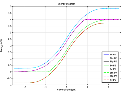
In the Model Builder window, expand the Energy Levels (semi) node, then click Conduction Band Energy Level.
2
In the Settings window for Line Graph, locate the x-Axis Data section.
3
From the Parameter list, choose Expression.
4
In the Expression text field, type x.
5
Click to expand the Legends section. In the table, enter the following settings:
Electron Quasi-Fermi Energy Level
1
In the Model Builder window, click Electron Quasi-Fermi Energy Level.
2
In the Settings window for Line Graph, locate the x-Axis Data section.
3
From the Parameter list, choose Expression.
4
In the Expression text field, type x.
5
Locate the Legends section. In the table, enter the following settings:
6
Click to expand the Coloring and Style section. Find the Line style subsection. From the Line list, choose Solid.
7
From the Color list, choose Gray.
Hole Quasi-Fermi Energy Level
1
In the Model Builder window, click Hole Quasi-Fermi Energy Level.
2
In the Settings window for Line Graph, locate the x-Axis Data section.
3
From the Parameter list, choose Expression.
4
In the Expression text field, type x.
5
Locate the Coloring and Style section. Find the Line style subsection. From the Line list, choose Solid.
6
Locate the Legends section. In the table, enter the following settings:
Valence Band Energy Level
1
In the Model Builder window, click Valence Band Energy Level.
2
In the Settings window for Line Graph, locate the x-Axis Data section.
3
From the Parameter list, choose Expression.
4
In the Expression text field, type x.
5
Locate the Legends section. In the table, enter the following settings:
Energy Levels Reverse Bias
1
In the Model Builder window, click Energy Levels (semi).
2
In the Settings window for 1D Plot Group, locate the Legend section.
3
From the Position list, choose Lower right.
4
In the Label text field, type Energy Levels Reverse Bias.
Carrier Concentrations Reverse Bias
1
In the Model Builder window, click Carrier Concentrations (semi).
2
In the Settings window for 1D Plot Group, locate the Legend section.
3
From the Position list, choose Lower right.
4
In the Label text field, type Carrier Concentrations Reverse Bias.
5
Locate the Data section. From the Parameter selection (bias) list, choose First.
6
From the Parameter selection (sweep) list, choose Last.
Electron Concentration
1
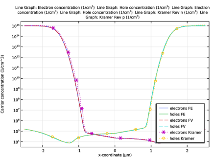
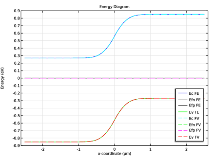
In the Model Builder window, expand the Carrier Concentrations Reverse Bias node, then click Electron Concentration.
2
In the Settings window for Line Graph, locate the x-Axis Data section.
3
From the Parameter list, choose Expression.
4
In the Expression text field, type x.
5
Locate the Legends section. In the table, enter the following settings:
Hole Concentration
1
In the Model Builder window, click Hole Concentration.
2
In the Settings window for Line Graph, locate the x-Axis Data section.
3
From the Parameter list, choose Expression.
4
In the Expression text field, type x.
5
Locate the Legends section. In the table, enter the following settings:
Line Graph 1
1
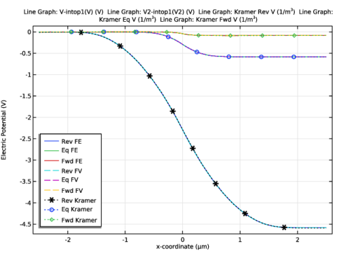
In the Model Builder window, expand the Results > Electric Potential (semi) node, then click Line Graph 1.
2
In the Settings window for Line Graph, locate the y-Axis Data section.
3
In the Expression text field, type V-intop1(V).
4
Locate the x-Axis Data section. From the Parameter list, choose Expression.
5
In the Expression text field, type x.
6
Locate the Legends section. Select the Show legends checkbox.
7
From the Legends list, choose Manual.
8
Electric Potential (semi)
1
In the Model Builder window, click Electric Potential (semi).
2
In the Settings window for 1D Plot Group, locate the Legend section.
3
From the Position list, choose Lower left.
4
Locate the Data section. From the Parameter selection (sweep) list, choose Last.
Net Dopant Concentration (semi)
1
In the Model Builder window, click Net Dopant Concentration (semi).
2
In the Settings window for 1D Plot Group, locate the Data section.
3
From the Parameter selection (bias) list, choose First.
4
From the Parameter selection (sweep) list, choose First.
5
In the Net Dopant Concentration (semi) toolbar, click  Plot.
In order to compare the finite element log formulation discretization with finite volume discretization, change the discretization and add a second study to re-solve the model with the new selection.
Add Study
1
In the Home toolbar, click  Add Study to open the Add Study window.
2
Go to the Add Study window.
3
Find the Studies subsection. In the Select Study tree, select General Studies > Stationary.
4
Click the Add Study button in the window toolbar.
5
In the Home toolbar, click  Add Study to close the Add Study window.
Study 2 - Finite Volume
1
In the Settings window for Study, type Study 2 - Finite Volume in the Label text field.
2
Locate the Study Settings section. Clear the Generate default plots checkbox.
Unlike in the previous study, the finite volume discretization does not require that the voltage be ramped up gradually. Therefore the desired values of ’Va’ can be set directly in the auxiliary sweep.
Step 1: Stationary
1
In the Model Builder window, under Study 2 - Finite Volume click Step 1: Stationary.
2
In the Settings window for Stationary, locate the Physics and Variables Selection section.
3
In the Solve for column of the table, under Component 1 (comp1), clear the checkbox for Semiconductor (semi).
4
Locate the Study Extensions section. Select the Auxiliary sweep checkbox.
5
6
7
In the Study toolbar, click  Compute.
Results
Line Graph 2
1
In the Model Builder window, under Results > Electric Potential (semi) right-click Line Graph 1 and choose Duplicate.
2
In the Settings window for Line Graph, locate the Data section.
3
From the Dataset list, choose Study 2 - Finite Volume/Solution 2 (sol2).
4
Locate the y-Axis Data section. In the Expression text field, type V2-intop1(V2).
5
Locate the Coloring and Style section. Find the Line style subsection. From the Line list, choose Dashed.
6
Locate the Legends section. In the table, enter the following settings:
Line Graph 3
1
Right-click Line Graph 1 and choose Duplicate.
2
In the Settings window for Line Graph, locate the y-Axis Data section.
3
In the Expression text field, type kramer_rev_V(x).
4
Locate the Data section. From the Dataset list, choose Study 1 - Finite Element Log Formulation/Solution 1 (sol1).
5
From the Parameter selection (bias) list, choose First.
6
From the Parameter selection (sweep) list, choose Last.
7
Locate the Coloring and Style section. Find the Line style subsection. From the Line list, choose Dotted.
8
Find the Line markers subsection. From the Marker list, choose Cycle.
9
Locate the Legends section. In the table, enter the following settings:
Line Graph 4
1
Right-click Line Graph 3 and choose Duplicate.
2
In the Settings window for Line Graph, locate the y-Axis Data section.
3
In the Expression text field, type kramer_eq_V(x).
4
Locate the Legends section. In the table, enter the following settings:
Line Graph 5
1
Right-click Line Graph 4 and choose Duplicate.
2
In the Settings window for Line Graph, locate the y-Axis Data section.
3
In the Expression text field, type kramer_fwd_V(x).
4
Locate the Legends section. In the table, enter the following settings:
5
In the Electric Potential (semi) toolbar, click  Plot.
Conduction Band Energy Level, Electron Quasi-Fermi Energy Level, Hole Quasi-Fermi Energy Level, Valence Band Energy Level
1
In the Model Builder window, under Results > Energy Levels Reverse Bias, Ctrl-click to select Conduction Band Energy Level, Electron Quasi-Fermi Energy Level, Hole Quasi-Fermi Energy Level, and Valence Band Energy Level.
2
Conduction Band Energy Level 1
1
In the Settings window for Line Graph, locate the Data section.
2
From the Dataset list, choose Study 2 - Finite Volume/Solution 2 (sol2).
3
From the Parameter selection (Va) list, choose First.
4
Locate the y-Axis Data section. In the Expression text field, type semi2.Ec_e.
5
Locate the Coloring and Style section. Find the Line style subsection. From the Line list, choose Dashed.
6
From the Color list, choose Cyan.
7
Locate the Legends section. In the table, enter the following settings:
Electron Quasi-Fermi Energy Level 1
1
In the Model Builder window, click Electron Quasi-Fermi Energy Level 1.
2
In the Settings window for Line Graph, locate the Data section.
3
From the Dataset list, choose Study 2 - Finite Volume/Solution 2 (sol2).
4
From the Parameter selection (Va) list, choose First.
5
Locate the y-Axis Data section. In the Expression text field, type semi2.Efn_e.
6
Locate the Coloring and Style section. Find the Line style subsection. From the Line list, choose Dashed.
7
From the Color list, choose Green.
8
Locate the Legends section. In the table, enter the following settings:
Hole Quasi-Fermi Energy Level 1
1
In the Model Builder window, click Hole Quasi-Fermi Energy Level 1.
2
In the Settings window for Line Graph, locate the Data section.
3
From the Dataset list, choose Study 2 - Finite Volume/Solution 2 (sol2).
4
From the Parameter selection (Va) list, choose First.
5
Locate the y-Axis Data section. In the Expression text field, type semi2.Efp_e.
6
Locate the Coloring and Style section. Find the Line style subsection. From the Line list, choose Dashed.
7
From the Color list, choose Magenta.
8
Locate the Legends section. In the table, enter the following settings:
Valence Band Energy Level 1
1
In the Model Builder window, click Valence Band Energy Level 1.
2
In the Settings window for Line Graph, locate the Data section.
3
From the Dataset list, choose Study 2 - Finite Volume/Solution 2 (sol2).
4
From the Parameter selection (Va) list, choose First.
5
Locate the y-Axis Data section. In the Expression text field, type semi2.Ev_e.
6
Locate the Coloring and Style section. Find the Line style subsection. From the Line list, choose Dashed.
7
From the Color list, choose Red.
8
Locate the Legends section. In the table, enter the following settings:
9
In the Energy Levels Reverse Bias toolbar, click  Plot.
Electron Concentration, Hole Concentration
1
In the Model Builder window, under Results > Carrier Concentrations Reverse Bias, Ctrl-click to select Electron Concentration and Hole Concentration.
2
Electron Concentration 1
1
In the Settings window for Line Graph, locate the Data section.
2
From the Dataset list, choose Study 2 - Finite Volume/Solution 2 (sol2).
3
From the Parameter selection (Va) list, choose First.
4
Locate the y-Axis Data section. In the Expression text field, type semi2.N.
5
Locate the Coloring and Style section. Find the Line style subsection. From the Line list, choose Dashed.
6
Locate the Legends section. In the table, enter the following settings:
Hole Concentration 1
1
In the Model Builder window, click Hole Concentration 1.
2
In the Settings window for Line Graph, locate the Data section.
3
From the Dataset list, choose Study 2 - Finite Volume/Solution 2 (sol2).
4
From the Parameter selection (Va) list, choose First.
5
Locate the y-Axis Data section. In the Expression text field, type semi2.P.
6
Locate the Coloring and Style section. Find the Line style subsection. From the Line list, choose Dashed.
7
Locate the Legends section. In the table, enter the following settings:
Electron Concentration 1, Hole Concentration 1
1
In the Model Builder window, under Results > Carrier Concentrations Reverse Bias, Ctrl-click to select Electron Concentration 1 and Hole Concentration 1.
2
Electron Concentration 1.1
1
In the Settings window for Line Graph, locate the y-Axis Data section.
2
In the Expression text field, type kramer_rev_n(x).
3
Locate the Coloring and Style section. Find the Line style subsection. From the Line list, choose Dotted.
4
Find the Line markers subsection. From the Marker list, choose Cycle.
5
Locate the Legends section. In the table, enter the following settings:
Hole Concentration 1.1
1
In the Model Builder window, click Hole Concentration 1.1.
2
In the Settings window for Line Graph, locate the y-Axis Data section.
3
In the Expression text field, type kramer_rev_p(x).
4
Locate the Coloring and Style section. Find the Line style subsection. From the Line list, choose Dotted.
5
Find the Line markers subsection. From the Marker list, choose Cycle.
6
Locate the Legends section. In the table, enter the following settings:
7
In the Carrier Concentrations Reverse Bias toolbar, click  Plot.
Carrier Concentrations Reverse Bias, Energy Levels Reverse Bias
1
In the Model Builder window, under Results, Ctrl-click to select Energy Levels Reverse Bias and Carrier Concentrations Reverse Bias.
2
Carrier Concentrations Reverse Bias 1, Energy Levels Reverse Bias 1
Right-click and choose Duplicate.
Energy Levels Equilibrium
1
In the Settings window for 1D Plot Group, type Energy Levels Equilibrium in the Label text field.
2
Locate the Data section. From the Parameter selection (sweep) list, choose From list.
3
In the Parameter values (sweep) list box, select 0.
Conduction Band Energy Level 1
1
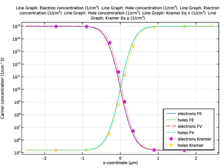
In the Model Builder window, expand the Energy Levels Equilibrium node, then click Conduction Band Energy Level 1.
2
In the Settings window for Line Graph, locate the Data section.
3
From the Parameter selection (Va) list, choose From list.
4
In the Parameter values (Va (V)) list box, select 0.
Electron Quasi-Fermi Energy Level 1
1
In the Model Builder window, click Electron Quasi-Fermi Energy Level 1.
2
In the Settings window for Line Graph, locate the Data section.
3
From the Parameter selection (Va) list, choose From list.
4
In the Parameter values (Va (V)) list box, select 0.
Hole Quasi-Fermi Energy Level 1
1
In the Model Builder window, click Hole Quasi-Fermi Energy Level 1.
2
In the Settings window for Line Graph, locate the Data section.
3
From the Parameter selection (Va) list, choose From list.
4
In the Parameter values (Va (V)) list box, select 0.
Valence Band Energy Level 1
1
In the Model Builder window, click Valence Band Energy Level 1.
2
In the Settings window for Line Graph, locate the Data section.
3
From the Parameter selection (Va) list, choose From list.
4
In the Parameter values (Va (V)) list box, select 0.
5
In the Energy Levels Equilibrium toolbar, click  Plot.
Carrier Concentrations Reverse Bias 1
1
In the Model Builder window, under Results click Carrier Concentrations Reverse Bias 1.
2
In the Settings window for 1D Plot Group, locate the Data section.
3
From the Parameter selection (sweep) list, choose From list.
4
In the Parameter values (sweep) list box, select 0.
Electron Concentration 1
1
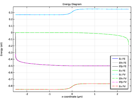
In the Model Builder window, expand the Carrier Concentrations Reverse Bias 1 node, then click Electron Concentration 1.
2
In the Settings window for Line Graph, locate the Data section.
3
From the Parameter selection (Va) list, choose From list.
4
In the Parameter values (Va (V)) list box, select 0.
Hole Concentration 1
1
In the Model Builder window, click Hole Concentration 1.
2
In the Settings window for Line Graph, locate the Data section.
3
From the Parameter selection (Va) list, choose From list.
4
In the Parameter values (Va (V)) list box, select 0.
Electron Concentration 1.1
1
In the Model Builder window, click Electron Concentration 1.1.
2
In the Settings window for Line Graph, locate the y-Axis Data section.
3
In the Expression text field, type kramer_eq_n(x).
Hole Concentration 1.1
1
In the Model Builder window, click Hole Concentration 1.1.
2
In the Settings window for Line Graph, locate the y-Axis Data section.
3
In the Expression text field, type kramer_eq_p(x).
4
In the Carrier Concentrations Reverse Bias 1 toolbar, click  Plot.
Carrier Concentrations Equilibrium
1
In the Model Builder window, right-click Carrier Concentrations Reverse Bias 1 and choose Rename.
2
In the Rename 1D Plot Group dialog, type Carrier Concentrations Equilibrium in the New label text field.
3
Energy Levels Reverse Bias 1.1
1
In the Model Builder window, click Energy Levels Reverse Bias 1.1.
2
In the Settings window for 1D Plot Group, locate the Data section.
3
From the Parameter selection (bias) list, choose Last.
Conduction Band Energy Level 1
1
In the Model Builder window, expand the Energy Levels Reverse Bias 1.1 node, then click Conduction Band Energy Level 1.
2
In the Settings window for Line Graph, locate the Data section.
3
From the Parameter selection (Va) list, choose Last.
Electron Quasi-Fermi Energy Level 1
1
In the Model Builder window, click Electron Quasi-Fermi Energy Level 1.
2
In the Settings window for Line Graph, locate the Data section.
3
From the Parameter selection (Va) list, choose Last.
Hole Quasi-Fermi Energy Level 1
1
In the Model Builder window, click Hole Quasi-Fermi Energy Level 1.
2
In the Settings window for Line Graph, locate the Data section.
3
From the Parameter selection (Va) list, choose Last.
Valence Band Energy Level 1
1
In the Model Builder window, click Valence Band Energy Level 1.
2
In the Settings window for Line Graph, locate the Data section.
3
From the Parameter selection (Va) list, choose Last.
4
In the Energy Levels Reverse Bias 1.1 toolbar, click  Plot.
Energy Levels Forward Bias
1
In the Model Builder window, right-click Energy Levels Reverse Bias 1.1 and choose Rename.
2
In the Rename 1D Plot Group dialog, type Energy Levels Forward Bias in the New label text field.
3
Carrier Concentrations Forward Bias
1
In the Model Builder window, under Results click Carrier Concentrations Reverse Bias 1.1.
2
In the Settings window for 1D Plot Group, type Carrier Concentrations Forward Bias in the Label text field.
3
Locate the Data section. From the Parameter selection (bias) list, choose Last.
Electron Concentration 1
1
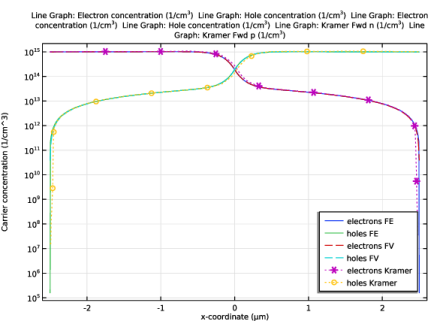
In the Model Builder window, expand the Carrier Concentrations Forward Bias node, then click Electron Concentration 1.
2
In the Settings window for Line Graph, locate the Data section.
3
From the Parameter selection (Va) list, choose Last.
Hole Concentration 1
1
In the Model Builder window, click Hole Concentration 1.
2
In the Settings window for Line Graph, locate the Data section.
3
From the Parameter selection (Va) list, choose Last.
Electron Concentration 1.1
1
In the Model Builder window, click Electron Concentration 1.1.
2
In the Settings window for Line Graph, locate the y-Axis Data section.
3
In the Expression text field, type kramer_fwd_n(x).
Hole Concentration 1.1
1
In the Model Builder window, click Hole Concentration 1.1.
2
In the Settings window for Line Graph, locate the y-Axis Data section.
3
In the Expression text field, type kramer_fwd_p(x).
4
In the Carrier Concentrations Forward Bias toolbar, click  Plot.