PDF

DC Characteristics of a MESFET
This model compares the current–voltage characteristics of a MESFET using the majority carrier only formulation.
Introduction
MOSFETs and MESFETs (metal–semiconductor field-effect transistor) work very similarly. In a MESFET, the gate forms a rectifying junction that controls the opening of the channel by varying the depletion width of the junction.
In this model we simulate the response of a n-doped GaAs MESFET to different drain and gate voltages. For a n-doped material the electron concentration is expected to be orders of magnitude larger than the hole concentration. Accordingly, it is possible to use the majority carrier option to compute an accurate solution with less degrees of freedom then it would normally be needed using the electrons and holes formulation.
Model Definition
The model compares the effect of the carrier formulation on the solution of a 2D MESFET biased with different gate (0, 1, and 2 V) and drain (from 0 to 10 V) voltages.
The geometry is composed of a block of 4 by 0.5 μm. The Schottky contact (gate) has a length of 1 μm. The source (top left) and drain (top right) have both a length of 0.5 μm. Figure 1 shows the model’s geometry.
Figure 1: Geometry of the modeled MESFET.
Results and Discussion
Figure 2 plots the drain current as a function of the drain voltage for both studies (electrons and holes and majority carrier only). The result is identical. Note that the number of degrees of freedom used for the first study (electrons and holes) is 1.5 times larger than the number of degrees of freedom used for the second study (majority carrier only).
Figure 2: Drain current as a function of the drain voltage for the electrons and holes and for the majority carrier only (asterisk).
Application Library path: Semiconductor_Module/Transistors/mesfet
Modeling Instructions
From the File menu, choose New.
New
In the New window, click  Model Wizard.
Model Wizard
1
In the Model Wizard window, click  2D.
2
In the Select Physics tree, select Semiconductor > Semiconductor (semi).
3
Click Add.
4
Global Definitions
Parameters 1
1
In the Model Builder window, under Global Definitions click Parameters 1.
2
In the Settings window for Parameters, locate the Parameters section.
3
Geometry 1
1
In the Model Builder window, under Component 1 (comp1) click Geometry 1.
2
In the Settings window for Geometry, locate the Units section.
3
From the Length unit list, choose µm.
Rectangle 1 (r1)
1
In the Geometry toolbar, click  Rectangle.
2
In the Settings window for Rectangle, locate the Size and Shape section.
3
In the Width text field, type Wd.
4
In the Height text field, type Hd.
5
Locate the Position section. In the x text field, type -Wd/2.
Add points to define the source, drain and gate contacts.
Point 1 (pt1)
1
In the Geometry toolbar, click  Point.
2
In the Settings window for Point, locate the Point section.
3
In the x text field, type -Wd/2+Ws/2 -L/2 L/2 Wd/2-Ws/2.
4
In the y text field, type Hd Hd Hd Hd.
5
Click  Build All Objects.
Add Material
1
In the Materials toolbar, click  Add Material to open the Add Material window.
2
Go to the Add Material window.
3
In the tree, select Semiconductors > GaAs - Gallium Arsenide.
4
Click the Add to Component button in the window toolbar.
5
In the Materials toolbar, click  Add Material to close the Add Material window.
Semiconductor (semi)
Metal Contact 1
1
In the Physics toolbar, click  Boundaries and choose Metal Contact.
2
In the Settings window for Metal Contact, locate the Contact Type section.
3
From the Type list, choose Ideal Schottky.
4
5
Locate the Terminal section. In the V0 text field, type -Vg.
Metal Contact 2
1
In the Physics toolbar, click  Boundaries and choose Metal Contact.
2
3
In the Settings window for Metal Contact, locate the Terminal section.
4
In the V0 text field, type Vs.
Metal Contact 3
1
In the Physics toolbar, click  Boundaries and choose Metal Contact.
2
3
In the Settings window for Metal Contact, locate the Terminal section.
4
In the V0 text field, type Vd.
Analytic Doping Model 1
1
In the Physics toolbar, click  Domains and choose Analytic Doping Model.
2
3
In the Settings window for Analytic Doping Model, locate the Impurity section.
4
From the Impurity type list, choose Donor doping (n-type).
5
In the ND0 text field, type Nd.
Trap-Assisted Recombination 1
1
In the Physics toolbar, click  Domains and choose Trap-Assisted Recombination.
2
3
In the Settings window for Trap-Assisted Recombination, locate the Shockley–Read–Hall Recombination section.
4
From the τn list, choose User defined. From the τp list, choose User defined. In the Model Builder window, right-click Semiconductor (semi) and choose Copy.
Semiconductor 2 (semi2)
1
In the Model Builder window, right-click Component 1 (comp1) and choose Paste Semiconductor.
2
In the Messages from Paste dialog, click OK.
3
In the Settings window for Semiconductor, locate the Model Properties section.
4
From the Solution list, choose Majority carriers only.
Adjust the mesh slightly.
Mesh 1
In the Model Builder window, under Component 1 (comp1) right-click Mesh 1 and choose Edit Physics-Induced Sequence.
Size 2
1
In the Model Builder window, under Component 1 (comp1) > Mesh 1 click Size 2.
2
In the Settings window for Size, locate the Element Size section.
3
From the Predefined list, choose Finer.
4
Click  Build All.
Add Study
1
In the Home toolbar, click  Add Study to open the Add Study window.
2
Go to the Add Study window.
3
Find the Studies subsection. In the Select Study tree, select General Studies > Stationary.
4
Click the Add Study button in the window toolbar.
5
In the Home toolbar, click  Add Study to close the Add Study window.
Study 1
Step 1: Stationary
1
In the Settings window for Stationary, locate the Physics and Variables Selection section.
2
In the Solve for column of the table, under Component 1 (comp1), clear the checkbox for Semiconductor 2 (semi2).
Set up an auxiliary continuation sweep for the ’Vd’ parameter.
3
Click to expand the Study Extensions section. Select the Auxiliary sweep checkbox.
4
5
6
7
8
From the Sweep type list, choose All combinations.
9
From the Reuse solution from previous step list, choose Auto.
10
In the Study toolbar, click  Compute.
Results
Net Dopant Concentration (semi)
The model has a uniform n-doping therefore, we remove the generated default plot, Net Dopant Concentration.
1
In the Model Builder window, under Results right-click Net Dopant Concentration (semi) and choose Delete.
Drain current as a function of drain voltage
1
In the Results toolbar, click  1D Plot Group.
2
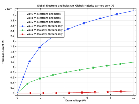
In the Settings window for 1D Plot Group, type Drain current as a function of drain voltage in the Label text field.
3
Locate the Legend section. From the Position list, choose Upper left.
Global 1
1
Right-click Drain current as a function of drain voltage and choose Global.
2
In the Settings window for Global, click Replace Expression in the upper-right corner of the y-Axis Data section. From the menu, choose Component 1 (comp1) > Semiconductor > Terminals > semi.I0_3 - Terminal current - A.
3
Locate the y-Axis Data section. In the table, enter the following settings:
4
In the Drain current as a function of drain voltage toolbar, click  Plot.
Add Study
1
In the Home toolbar, click  Add Study to open the Add Study window.
2
Go to the Add Study window.
3
Find the Studies subsection. In the Select Study tree, select General Studies > Stationary.
4
Click the Add Study button in the window toolbar.
5
In the Home toolbar, click  Add Study to close the Add Study window.
Study 2
Step 1: Stationary
1
In the Settings window for Stationary, locate the Physics and Variables Selection section.
2
In the Solve for column of the table, under Component 1 (comp1), clear the checkbox for Semiconductor (semi).
3
Locate the Study Extensions section. Select the Auxiliary sweep checkbox.
4
5
6
7
8
From the Sweep type list, choose All combinations.
9
From the Reuse solution from previous step list, choose Auto.
10
In the Study toolbar, click  Compute.
Results
Net Dopant Concentration (semi2)
The model has a uniform n-doping therefore, we remove the generated default plot, Net Dopant Concentration.
1
In the Model Builder window, under Results right-click Net Dopant Concentration (semi2) and choose Delete.
Global 2
1
In the Model Builder window, under Results > Drain current as a function of drain voltage right-click Global 1 and choose Duplicate.
2
In the Settings window for Global, locate the Data section.
3
From the Dataset list, choose Study 2/Solution 2 (sol2).
4
Click Replace Expression in the upper-right corner of the y-Axis Data section. From the menu, choose Component 1 (comp1) > Semiconductor 2 > Terminals > semi2.I0_3 - Terminal current - A.
5
Locate the y-Axis Data section. In the table, enter the following settings:
6
Click to expand the Coloring and Style section. Find the Line markers subsection. From the Marker list, choose Asterisk.
7
From the Positioning list, choose Interpolated.
8
Click to expand the Coloring and Style section. From the Color list, choose Cycle (reset).
Drain current as a function of drain voltage
1
In the Model Builder window, click Drain current as a function of drain voltage.
2
In the Settings window for 1D Plot Group, locate the Plot Settings section.
3
Select the x-axis label checkbox. In the associated text field, type Drain voltage (V).
4
Select the y-axis label checkbox. In the associated text field, type Terminal current (A).
5
In the Drain current as a function of drain voltage toolbar, click  Plot.