PDF

Simulation of an Ion-Sensitive Field-Effect Transistor (ISFET)
This tutorial uses a 2D model of an ion-sensitive field-effect transistor (ISFET) to illustrate the basic steps to set up the coupling between semiconductor physics and electrochemistry.
Introduction
An ion-sensitive field-effect transistor (ISFET) is constructed by replacing the gate contact of a MOSFET with an electrolyte of interest. The concentration of a specific ionic species in the electrolyte can be determined by measuring the change in the gate voltage due to the interaction between the ions and the gate dielectric. This tutorial of an ISFET pH sensor illustrates the procedure to set up the coupling between the semiconductor model and the electrolyte model. It also shows the technique of using a simple global equation to extract operating parameters without the need of explicit modeling of the actual feedback circuitry.
Model Definition
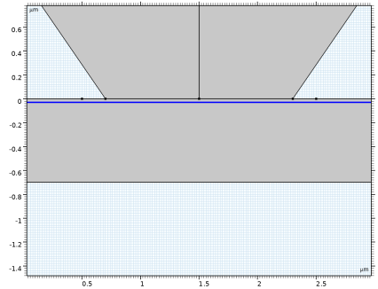
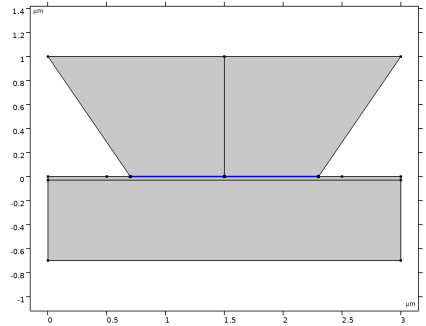
The model is composed of essentially two adjacent domains: a semiconductor domain and an electrolyte domain. (The electrolyte domain is split in half along the centerline of the geometry for convenience in making some graphs.) The semiconductor domain is set up as a MOSFET. The thin oxide layer is not explicitly modeled — the dedicated Thin Insulator Gate boundary condition is used instead. Unlike a conventional MOSFET, the electric potential at the outer surface of the oxide (phiM) is not given by the potential of a metal contact; rather, it is given by the electric potential of the electrolyte just outside of the Stern layer, plus the voltage drop across the Stern layer, following the same treatment as in the Diffuse Double Layer tutorial.
The electrolyte domain is set up in the same way as the Diffuse Double Layer tutorial except that the Transport of Charge Carriers interface is used instead, with the addition of hydronium and hydroxide ions. The Stern layer is not explicitly modeled — a simple formula relating the electric potential on each side of the Stern layer is used instead. The bulk electrolyte potential is given by a simple formula combining the gate voltage applied on the reference electrode (not explicitly modeled), the work function of the electrode metal, and the equilibrium potential of the reference electrode. Unlike in the tutorial, the value of the electric potential at the outer surface of the oxide (phiM) is not given by a prescribed constant; rather, it is solved for in a self-consistent manner. The self-consistent set of equations include essentially three parts:
phiM is the sum of the voltage drop across the Stern layer and the electrolyte potential just outside of the Stern layer.
The coupling between the semiconductor and the electrolyte domain is implemented as the following. For the semiconductor domain, the electric potential phiM is imposed on the oxide surface. For the electrolyte domain, the displacement field is determined from the charge density on the oxide surface and the displacement field on the semiconductor side using Gauss’ law, and imposed on the boundary. Note that it is assumed that there is no space charge in the Stern layer; therefore, the displacement field does not change across the Stern layer.
As the fully coupled system is highly nonlinear, individual studies are set up in a sequence to solve different aspects of the system step by step, using the solution from each previous study as the initial condition for the next study. First only the electrolyte part is solved. Then the semiconductor part is solved. Then the fully coupled system is solved in three different scenarios, to examine:
1
2
3
Results and Discussion
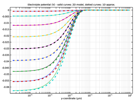
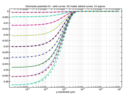
Figure 1 shows the electrolyte potential along the centerline of the electrolyte domain, comparing the simulation result (solid curves) and the 1D approximation formula (dotted curves; Ref. 1). The 1D approximation formula matches the general trend of the 2D model result.
.
Figure 1: Electrolyte potential along the centerline of the electrolyte domain. (It does not extrapolate to the dielectric surface potential at y=0 because the voltage drop across the Stern layer is not explicitly modeled in the electrolyte domain. See Model Definition for details.)
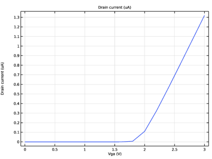
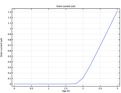
Figure 2 shows the drain current as a function of the gate voltage for the fully coupled system. The behavior of this Id–Vg curve is essentially the same as a regular MOSFET. This is expected since the electrolyte acts as a conductor to transmit the applied voltage to the oxide surface, albeit with a more complicated mechanism than a simple metal contact.
Figure 2: Drain current as a function of the applied gate voltage.
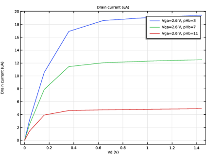
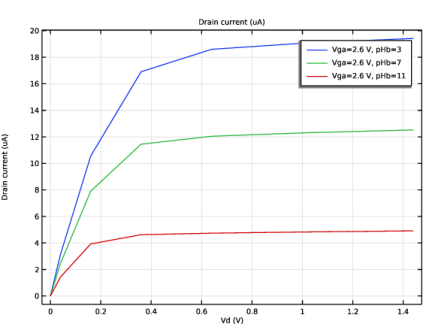
Figure 3 shows the drain current–drain voltage curves for three different pH values. Again the behavior of the family of curves looks just like a regular MOSFET, except for the fact that in a regular MOSFET the control parameter is the gate voltage but here the control parameter is the pH value.
Figure 3: Drain current–drain voltage curves for three different pH values.
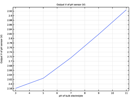
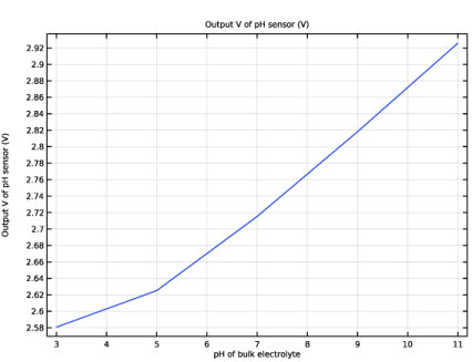
Figure 4 shows the sensitivity curve for the ISFET pH sensor operating in the constant-current mode, where a feedback circuit adjusts the applied gate voltage such that the drain current is maintained at a constant set point. The resulting gate voltage (the output of the sensor) as a function of the pH value (the input of the sensor) is plotted in the figure. The slope of the curve gives the sensitivity, which is consistent with the one reported in Ref. 1.
Figure 4: Sensitivity curve for the ISFET pH sensor.
Reference
1. R.E.G. van Hal, J.C.T. Eijkel, P. Bergveld, A general model to describe the electrostatic potential at electrolyte oxide interfaces, Advances in Colloid and Interface Science, Volume 69, Issue 1, 1996, Pages 31-62, ISSN 0001-8686, http://dx.doi.org/10.1016/S0001-8686(96)00307-7.(http://www.sciencedirect.com/science/article/pii/S0001868696003077)
Application Library path: Semiconductor_Module/Photonic_Devices_and_Sensors/isfet
Modeling Instructions
From the File menu, choose New.
New
In the New window, click  Model Wizard.
Model Wizard
1
In the Model Wizard window, click  2D.
2
In the Select Physics tree, select Semiconductor > Semiconductor (semi).
3
Click Add.
4
Studies will be added later.
Geometry 1
The Model Wizard starts the COMSOL Desktop with the Geometry node selected. Take the opportunity to set the length unit to a more convenient one.
1
In the Model Builder window, under Component 1 (comp1) click Geometry 1.
2
In the Settings window for Geometry, locate the Units section.
3
From the Length unit list, choose µm.
Now import some global parameters from a text file.
Global Definitions
Parameters 1
1
In the Model Builder window, under Global Definitions click Parameters 1.
2
In the Settings window for Parameters, locate the Parameters section.
3
Click  Load from File.
4
Next build the geometric objects in the model.
Geometry 1
Rectangle 1 (r1)
1
In the Geometry toolbar, click  Rectangle.
2
In the Settings window for Rectangle, locate the Size and Shape section.
3
In the Width text field, type 3.
4
In the Height text field, type 0.7.
5
Locate the Position section. In the y text field, type -0.7.
Polygon 1 (pol1)
1
In the Geometry toolbar, click  Polygon.
2
In the Settings window for Polygon, locate the Object Type section.
3
From the Type list, choose Closed curve.
4
Locate the Coordinates section. In the table, enter the following settings:
Polygon 2 (pol2)
1
In the Geometry toolbar, click  Polygon.
2
In the Settings window for Polygon, locate the Coordinates section.
3
Polygon 3 (pol3)
1
In the Geometry toolbar, click  Polygon.
2
In the Settings window for Polygon, locate the Object Type section.
3
From the Type list, choose Open curve.
4
Locate the Coordinates section. In the table, enter the following settings:
Mesh Control Edges 1 (mce1)
1
In the Geometry toolbar, click  Virtual Operations and choose Mesh Control Edges.
2
On the object fin, select Boundary 4 only.
It might be easier to select the correct boundary by using the Selection List window. To open this window, in the Home toolbar click Windows and choose Selection List. (If you are running the cross-platform desktop, you find Windows in the main menu.)
Define some variables to be used in various stages of the model setup.
Definitions
Variables for applying specified gate voltage (Vg)
1
In the Model Builder window, under Component 1 (comp1) right-click Definitions and choose Variables.
2
In the Settings window for Variables, type Variables for applying specified gate voltage (Vg) in the Label text field.
3
Locate the Variables section. In the table, enter the following settings:
Variables for adjusting Vg to obtain specified drain current
1
Right-click Variables for applying specified gate voltage (Vg) and choose Duplicate.
2
In the Settings window for Variables, type Variables for adjusting Vg to obtain specified drain current in the Label text field.
3
Locate the Variables section. In the table, enter the following settings:
Variables on oxide surface
1
In the Model Builder window, right-click Definitions and choose Variables.
2
In the Settings window for Variables, type Variables on oxide surface in the Label text field.
3
Locate the Geometric Entity Selection section. From the Geometric entity level list, choose Boundary.
4
5
Locate the Variables section. In the table, enter the following settings:
Some expressions entered so far may contain undefined variables and turn to yellow color. The missing variables will be defined later and the color for the expressions will turn back to black.
Define materials.
Add Material
1
In the Home toolbar, click  Add Material to open the Add Material window.
2
Go to the Add Material window.
3
In the tree, select Semiconductors > Si - Silicon.
4
Click the Add to Component button in the window toolbar.
5
In the Home toolbar, click  Add Material to close the Add Material window.
Materials
Electrolyte
1
In the Model Builder window, under Component 1 (comp1) right-click Materials and choose Blank Material.
2
In the Settings window for Material, type Electrolyte in the Label text field.
3
4
Locate the Geometric Entity Selection section. Click  Create Selection.
5
In the Create Selection dialog, type Electrolyte domains in the Selection name text field.
6
7
In the Settings window for Material, locate the Material Contents section.
8
So far all domains are assigned to the Semiconductor interface. Therefore, there are red marks for the electrolyte material properties. Once the proper physics is assigned to the electrolyte domain, the unnecessary material property entries and the red marks should disappear.
Set up the semiconductor domain and boundary conditions, similar to the MOSFET tutorial in the Application Libraries.
Semiconductor (semi)
1
In the Model Builder window, under Component 1 (comp1) click Semiconductor (semi).
2
3
In the Settings window for Semiconductor, locate the Model Properties section.
4
From the Carrier statistics list, choose Fermi–Dirac.
Semiconductor Material Model 1
1
In the Model Builder window, under Component 1 (comp1) > Semiconductor (semi) click Semiconductor Material Model 1.
2
In the Settings window for Semiconductor Material Model, locate the Model Input section.
3
In the T text field, type T0.
Uniform background doping
1
In the Physics toolbar, click  Domains and choose Analytic Doping Model.
2
In the Settings window for Analytic Doping Model, type Uniform background doping in the Label text field.
3
4
Locate the Impurity section. In the NA0 text field, type 1e17[1/cm^3].
Source doping
1
In the Physics toolbar, click  Domains and choose Analytic Doping Model.
2
In the Settings window for Analytic Doping Model, type Source doping in the Label text field.
3
4
Locate the Distribution section. From the list, choose Box.
5
Locate the Impurity section. From the Impurity type list, choose Donor doping (n-type).
6
In the ND0 text field, type 1e20[1/cm^3].
7
Locate the Uniform Region section. Specify the r0 vector as
8
In the W text field, type 0.6[um].
9
In the D text field, type 0.1[um].
10
Locate the Profile section. Select the Specify different length scales for each direction checkbox.
11
Specify the dj vector as
The background doping level for the junction profile can be conveniently set to the uniform background doping level that you just defined, using the Background doping concentration list.
12
From the Nb list, choose Acceptor concentration (semi/adm1).
13
To see which item in the list corresponds to which node in the model tree, toggle on the Tag setting in the Model Tree Node Text menu in the Model Builder window toolbar.
Drain doping
1
Right-click Source doping and choose Duplicate.
2
In the Settings window for Analytic Doping Model, type Drain doping in the Label text field.
3
Locate the Uniform Region section. Specify the r0 vector as
Trap-Assisted Recombination 1
1
In the Physics toolbar, click  Domains and choose Trap-Assisted Recombination.
2
Source
1
In the Physics toolbar, click  Boundaries and choose Metal Contact.
2
In the Settings window for Metal Contact, type Source in the Label text field.
3
Drain
1
In the Physics toolbar, click  Boundaries and choose Metal Contact.
2
In the Settings window for Metal Contact, type Drain in the Label text field.
3
4
Locate the Terminal section. In the V0 text field, type Vd.
Body
1
In the Physics toolbar, click  Boundaries and choose Metal Contact.
2
In the Settings window for Metal Contact, type Body in the Label text field.
3
Thin Insulator Gate 1
1
In the Physics toolbar, click  Boundaries and choose Thin Insulator Gate.
2
3
In the Settings window for Thin Insulator Gate, locate the Terminal section.
4
In the V0 text field, type phiM.
5
Locate the Gate Contact section. In the εins text field, type 4.5.
6
In the dins text field, type 30[nm].
7
In the Φ text field, type 0[V].
The undefined variable phiM will be defined later.
Add Physics
1
In the Physics toolbar, click  Add Physics to open the Add Physics window.
2
Go to the Add Physics window.
3
In the tree, select AC/DC > Electric Fields and Currents > Electrostatics (es).
4
Click to expand the Dependent Variables section. In the Electric potential (V) text field, type phil.
5
Click the Add to Component 1 button in the window toolbar.
Electrostatics (es)
1
In the Settings window for Electrostatics, locate the Domain Selection section.
2
From the Selection list, choose Electrolyte domains.
Add Physics
1
Go to the Add Physics window.
2
In the tree, select Electric Discharge > Transport of Charge Carriers (tcc).
3
Click the Add to Component 1 button in the window toolbar.
Transport of Charge Carriers (electrolyte)
1
In the Settings window for Transport of Charge Carriers, type Transport of Charge Carriers (electrolyte) in the Label text field.
2
Locate the Domain Selection section. In the list box, select 1.
3
Click  Remove from Selection.
4
5
From the Selection list, choose Electrolyte domains.
6
Locate the Physical Model section. In the dz text field, type 1[m].
7
Click to expand the Dependent Variables section. In the Number of charge carriers text field, type 4.
8
In the Charge carriers (1/m³) table, enter the following settings:
Add Physics
1
Go to the Add Physics window.
2
In the tree, select Mathematics > ODE and DAE Interfaces > Boundary ODEs and DAEs (bode).
3
Click to expand the Dependent Variables section. In the Dependent variables (1) table, enter the following settings:
4
Click the Add to Component 1 button in the window toolbar.
Boundary ODEs and DAEs (bode)
1
In the Settings window for Boundary ODEs and DAEs, locate the Boundary Selection section.
2
Click  Clear Selection.
3
Add Physics
1
Go to the Add Physics window.
2
In the tree, select Mathematics > ODE and DAE Interfaces > Global ODEs and DAEs (ge).
3
Click the Add to Component 1 button in the window toolbar.
4
In the tree, select Mathematics > ODE and DAE Interfaces > Global ODEs and DAEs (ge).
5
Click the Add to Component 1 button in the window toolbar.
6
In the Home toolbar, click  Add Physics to close the Add Physics window.
Electrostatics (electrolyte)
1
In the Settings window for Electrostatics, type Electrostatics (electrolyte) in the Label text field.
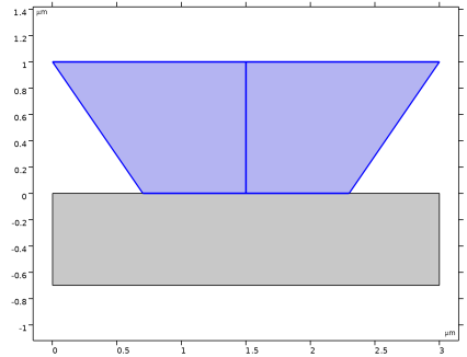
2
Locate the Thickness section. In the d text field, type 1e-6[m].
Charge Conservation in Fluids 1
1
In the Physics toolbar, click  Domains and choose Charge Conservation in Fluids.
2
In the Settings window for Charge Conservation in Fluids, locate the Domain Selection section.
3
From the Selection list, choose Electrolyte domains.
Boundary ODE for oxide surface potential phiM
1
In the Model Builder window, under Component 1 (comp1) click Boundary ODEs and DAEs (bode).
2
In the Settings window for Boundary ODEs and DAEs, type Boundary ODE for oxide surface potential phiM in the Label text field.
3
Locate the Units section. Click  Select Dependent Variable Quantity.
4
In the Physical Quantity dialog, type electricpotential in the text field.
5
In the tree, select Electromagnetics > Electric potential (V).
6
7
In the Settings window for Boundary ODEs and DAEs, locate the Units section.
8
Click  Select Source Term Quantity.
9
In the Physical Quantity dialog, type electricpotential in the text field.
10
In the tree, select Electromagnetics > Electric potential (V).
11
Global ODE to copy specified Vg value
1
In the Model Builder window, under Component 1 (comp1) click Global ODEs and DAEs (ge).
2
In the Settings window for Global ODEs and DAEs, type Global ODE to copy specified Vg value in the Label text field.
Global ODE to adjust Vg for specified drain current
1
In the Model Builder window, under Component 1 (comp1) click Global ODEs and DAEs 2 (ge2).
2
In the Settings window for Global ODEs and DAEs, type Global ODE to adjust Vg for specified drain current in the Label text field.
Toggle off the Add Physics window.
Set up the electrostatics physics for the electrolyte.
Electrostatics (electrolyte) (es)
In the Model Builder window, under Component 1 (comp1) click Electrostatics (electrolyte) (es).
Electric Potential 1
1
In the Physics toolbar, click  Boundaries and choose Electric Potential.
2
3
In the Settings window for Electric Potential, locate the Electric Potential section.
4
In the V0 text field, type phil_bulk_g.
Electric Potential 2
1
In the Physics toolbar, click  Boundaries and choose Electric Potential.
2
3
In the Settings window for Electric Potential, locate the Electric Potential section.
4
In the V0 text field, type phil_bulk_d.
Electric Displacement Field from semiconductor side
1
In the Physics toolbar, click  Boundaries and choose Electric Displacement Field.
2
In the Settings window for Electric Displacement Field, type Electric Displacement Field from semiconductor side in the Label text field.
3
4
Locate the Electric Displacement Field section. Specify the D0 vector as
Surface Charge Density 1
1
In the Physics toolbar, click  Boundaries and choose Surface Charge Density.
2
3
In the Settings window for Surface Charge Density, locate the Surface Charge Density section.
4
In the ρs text field, type rhos0_g.
Surface Charge Density 2
1
In the Physics toolbar, click  Boundaries and choose Surface Charge Density.
2
3
In the Settings window for Surface Charge Density, locate the Surface Charge Density section.
4
In the ρs text field, type rhos0_d.
Space Charge Density 1
1
In the Physics toolbar, click  Domains and choose Space Charge Density.
2
In the Settings window for Space Charge Density, locate the Domain Selection section.
3
From the Selection list, choose All domains.
4
Locate the Space Charge Density section. From the ρv list, choose Space charge density (tcc/tp1).
Set up the transport physics for the electrolyte.
Transport of Charge Carriers (electrolyte) (tcc)
Transport Properties 1
1
In the Model Builder window, under Component 1 (comp1) > Transport of Charge Carriers (electrolyte) (tcc) click Transport Properties 1.
2
In the Settings window for Transport Properties, locate the Electric Field section.
3
From the E list, choose Electric field (es).
4
Locate the Drift section. In the zC text field, type zC.
5
In the zA text field, type zA.
6
In the zH text field, type 1.
7
In the zOH text field, type -1.
8
In the μC text field, type DC*F_const/(R_const*T0).
9
In the μA text field, type DA*F_const/(R_const*T0).
10
In the μH text field, type DH*F_const/(R_const*T0).
11
In the μOH text field, type DOH*F_const/(R_const*T0).
12
Locate the Diffusion section. In the DC text field, type DC.
13
In the DA text field, type DA.
14
In the DH text field, type DH.
15
In the DOH text field, type DOH.
Initial Values 1
1
In the Model Builder window, click Initial Values 1.
2
In the Settings window for Initial Values, locate the Initial Values section.
3
In the nC text field, type cC_bulk*N_A_const.
4
In the nA text field, type cA_bulk*N_A_const.
5
In the nH text field, type cH_bulk*N_A_const.
6
In the nOH text field, type cOH_bulk*N_A_const.
No Flux 1
1
In the Physics toolbar, click  Boundaries and choose No Flux.
2
In the Settings window for No Flux, locate the Boundary Selection section.
3
From the Selection list, choose All boundaries.
Number Density 1
1
In the Physics toolbar, click  Boundaries and choose Number Density.
2
In the Settings window for Number Density, locate the Boundary Selection section.
3
Click  Paste Selection.
4
In the Paste Selection dialog, type 5 10 in the Selection text field.
5
6
In the Settings window for Number Density, locate the Number Density section.
7
Select the Carrier C checkbox.
8
In the n0,C text field, type cC_bulk*N_A_const.
9
Select the Carrier A checkbox.
10
In the n0,A text field, type cA_bulk*N_A_const.
11
Select the Carrier H checkbox.
12
In the n0,H text field, type cH_bulk*N_A_const.
13
Select the Carrier OH checkbox.
14
In the n0,OH text field, type cOH_bulk*N_A_const.
Set up the boundary equation at the oxide surface. This couples the electric potential at the surface of the oxide to the electrolyte potential just outside of the Stern layer.
Boundary ODE for oxide surface potential phiM (bode)
Distributed ODE 1
1
In the Model Builder window, under Component 1 (comp1) > Boundary ODE for oxide surface potential phiM (bode) click Distributed ODE 1.
2
In the Settings window for Distributed ODE, locate the Source Term section.
3
In the f text field, type phil+es.nD/Ci_st-phiM.
4
Locate the Damping or Mass Coefficient section. In the da text field, type 0.
Initial Values 1
1
In the Model Builder window, click Initial Values 1.
2
In the Settings window for Initial Values, locate the Initial Values section.
3
In the phiM text field, type phil_bulk_g-0.01[V].
Initial Values 2
1
Right-click Component 1 (comp1) > Boundary ODE for oxide surface potential phiM (bode) > Initial Values 1 and choose Duplicate.
2
In the Settings window for Initial Values, locate the Initial Values section.
3
In the phiM text field, type phil_bulk_d-0.01[V].
Set up the two global equations for the gate voltage. Depending on the goal of each study, at most one of the two will be used at the same time.
Global ODE to copy specified Vg value (ge)
Global Equations 1 (ODE1)
1
In the Model Builder window, under Component 1 (comp1) > Global ODE to copy specified Vg value (ge) click Global Equations 1 (ODE1).
2
In the Settings window for Global Equations, locate the Global Equations section.
3
4
Locate the Units section. Click  Select Dependent Variable Quantity.
5
In the Physical Quantity dialog, type electricpotential in the text field.
6
In the tree, select Electromagnetics > Electric potential (V).
7
Global ODE to adjust Vg for specified drain current (ge2)
Global Equations 1 (ODE2)
1
In the Model Builder window, under Component 1 (comp1) > Global ODE to adjust Vg for specified drain current (ge2) click Global Equations 1 (ODE2).
2
In the Settings window for Global Equations, locate the Units section.
3
Click  Select Dependent Variable Quantity.
4
In the Physical Quantity dialog, type electricpotential in the text field.
5
In the tree, select Electromagnetics > Electric potential (V).
6
7
In the Settings window for Global Equations, locate the Global Equations section.
8
Construct the mesh. Use Mapped mesh and Boundary Layers to minimize the number of mesh elements while keeping the required resolution near the oxide surface.
Mesh 1
1
In the Model Builder window, under Component 1 (comp1) click Mesh 1.
2
In the Settings window for Mesh, locate the Sequence Type section.
3
From the list, choose User-controlled mesh.
Size
1
In the Model Builder window, under Component 1 (comp1) > Mesh 1 click Size.
2
In the Settings window for Size, locate the Element Size section.
3
Click the Custom button.
4
Locate the Element Size Parameters section. In the Maximum element size text field, type h_max.
Size 1
1
In the Model Builder window, click Size 1.
2
In the Settings window for Size, locate the Element Size section.
3
Click the Custom button.
4
Locate the Element Size Parameters section.
5
Select the Maximum element growth rate checkbox. In the associated text field, type 1.05.
Size 2
In the Model Builder window, right-click Size 2 and choose Delete.
Size 3
Right-click Size 3 and choose Delete.
Free Triangular 1
Right-click Free Triangular 1 and choose Delete.
Edge 1
1
In the Mesh toolbar, click  More Generators and choose Edge.
2
3
In the Settings window for Edge, click to expand the Control Entities section.
4
From the Smooth across removed control entities list, choose Off.
Size 1
1
Right-click Edge 1 and choose Size.
2
In the Settings window for Size, locate the Element Size section.
3
From the Calibrate for list, choose Semiconductor.
4
Click the Custom button.
5
Locate the Element Size Parameters section.
6
Select the Maximum element size checkbox. In the associated text field, type 0.03.
Mapped 1
1
In the Mesh toolbar, click  Mapped.
2
In the Settings window for Mapped, locate the Domain Selection section.
3
From the Geometric entity level list, choose Domain.
4
5
Click to expand the Control Entities section. From the Smooth across removed control entities list, choose Off.
6
Click to expand the Reduce Element Skewness section. Select the Adjust edge mesh checkbox.
Distribution 1
1
Right-click Mapped 1 and choose Distribution.
2
3
In the Settings window for Distribution, locate the Distribution section.
4
From the Distribution type list, choose Predefined.
5
In the Number of elements text field, type 8.
6
In the Element ratio text field, type 9.
7
From the Growth rate list, choose Exponential.
8
Select the Reverse direction checkbox.
Free Triangular 1
1
In the Mesh toolbar, click  Free Triangular.
2
In the Settings window for Free Triangular, locate the Domain Selection section.
3
From the Geometric entity level list, choose Domain.
4
5
Click to expand the Control Entities section. From the Smooth across removed control entities list, choose Off.
Boundary Layers 1
1
In the Mesh toolbar, click  Boundary Layers.
2
In the Settings window for Boundary Layers, locate the Domain Selection section.
3
From the Geometric entity level list, choose Domain.
4
From the Selection list, choose Electrolyte domains.
Boundary Layer Properties
1
In the Model Builder window, click Boundary Layer Properties.
2
3
In the Settings window for Boundary Layer Properties, locate the Layers section.
4
In the Number of layers text field, type 20.
5
In the Stretching factor text field, type 1.3.
6
From the Thickness specification list, choose First layer.
7
In the Thickness text field, type h_max_surf.
Now set up the studies. First let us only look at the electrolyte.
Add Study
1
In the Home toolbar, click  Add Study to open the Add Study window.
2
Go to the Add Study window.
3
Find the Physics interfaces in study subsection. In the table, clear the Solve checkboxes for Semiconductor (semi), Global ODE to copy specified Vg value (ge), and Global ODE to adjust Vg for specified drain current (ge2).
4
Find the Studies subsection. In the Select Study tree, select General Studies > Stationary.
5
Click the Add Study button in the window toolbar.
Study 1
Step 1: Stationary
1
In the Settings window for Stationary, locate the Physics and Variables Selection section.
2
Select the Modify model configuration for study step checkbox.
3
In the tree, select Component 1 (comp1) > Definitions > Variables for adjusting Vg to obtain specified drain current.
4
Click  Disable.
5
In the tree, select Component 1 (comp1) > Electrostatics (electrolyte) (es) > Electric Potential 2.
6
Click  Disable.
7
In the tree, select Component 1 (comp1) > Electrostatics (electrolyte) (es) > Electric Displacement Field from semiconductor side.
8
Click  Disable.
9
In the tree, select Component 1 (comp1) > Electrostatics (electrolyte) (es) > Surface Charge Density 2.
10
Click  Disable.
11
In the tree, select Component 1 (comp1) > Boundary ODE for oxide surface potential phiM (bode) > Initial Values 2.
12
Click  Disable.
13
In the tree, select Component 1 (comp1) > Global ODE to adjust Vg for specified drain current (ge2).
14
Click  Disable in Model.
It is necessary to disable one of the global equations because they share the same dependent variable name (Vg).
15
Click to expand the Study Extensions section. Select the Auxiliary sweep checkbox.
16
17
18
In the Model Builder window, click Study 1.
19
In the Settings window for Study, type Electrolyte only in the Label text field.
20
Locate the Study Settings section. Clear the Generate default plots checkbox.
21
In the Study toolbar, click  Compute.
The result can be compared to the one from the 1D approximation formula. First evaluate a list of electrolyte potentials to plug into the 1D approximation formula.
Results
Point Evaluation 1
1
In the Model Builder window, expand the Results node.
2
Right-click Results > Derived Values and choose Point Evaluation.
3
4
In the Settings window for Point Evaluation, locate the Expressions section.
5
6
Click  Evaluate.
Table 1
1
Go to the Table 1 window.
2
Click the Copy Table and Headers to Clipboard button in the window toolbar.
Paste the table content into a text editor. Format the column of electrolyte potential values into a single line. Copy the line of electrolyte potential values to paste into the Auxiliary Sweep parameter table in the next study step (see below).
Add Study
1
Go to the Add Study window.
2
Find the Physics interfaces in study subsection. In the table, clear the Solve checkboxes for Semiconductor (semi), Electrostatics (electrolyte) (es), Transport of Charge Carriers (electrolyte) (tcc), Boundary ODE for oxide surface potential phiM (bode), Global ODE to copy specified Vg value (ge), and Global ODE to adjust Vg for specified drain current (ge2).
3
Find the Studies subsection. In the Select Study tree, select Preset Studies for Selected Physics Interfaces > Stationary.
4
Click the Add Study button in the window toolbar.
Study 2
Step 1: Stationary
1
In the Settings window for Stationary, locate the Physics and Variables Selection section.
2
Select the Modify model configuration for study step checkbox.
3
In the tree, select Component 1 (comp1) > Definitions > Variables for adjusting Vg to obtain specified drain current.
4
Click  Disable.
5
In the tree, select Component 1 (comp1) > Definitions > Variables on oxide surface.
6
Click  Disable.
7
In the tree, select Component 1 (comp1) > Electrostatics (electrolyte) (es) > Electric Potential 2.
8
Click  Disable.
9
In the tree, select Component 1 (comp1) > Electrostatics (electrolyte) (es) > Surface Charge Density 2.
10
Click  Disable.
11
In the tree, select Component 1 (comp1) > Boundary ODE for oxide surface potential phiM (bode) > Initial Values 2.
12
Click  Disable.
13
In the tree, select Component 1 (comp1) > Global ODE to adjust Vg for specified drain current (ge2).
14
Click  Disable in Model.
15
Locate the Study Extensions section. Select the Auxiliary sweep checkbox.
16
17
Now paste the line of electrolyte potential values into the Auxiliary Sweep parameter table, as shown below.
18
19
In the Model Builder window, click Study 2.
20
In the Settings window for Study, type 1D approx for electrolyte only in the Label text field.
21
Locate the Study Settings section. Clear the Generate default plots checkbox.
22
In the Study toolbar, click  Compute.
Now, create a plot to compare the 2D model result to the 1D approximation formula.
Results
phil: 2D Model vs. 1D Approx.
1
In the Results toolbar, click  1D Plot Group.
2
In the Settings window for 1D Plot Group, type phil: 2D Model vs. 1D Approx. in the Label text field.
3
Click to expand the Title section. From the Title type list, choose Manual.
4
In the Title text area, type Electrolyte potential (V) - solid curves: 2D model, dotted curves: 1D approx..
Line Graph: 2D model
1
Right-click phil: 2D Model vs. 1D Approx. and choose Line Graph.
2
In the Settings window for Line Graph, type Line Graph: 2D model in the Label text field.
3
4
Locate the y-Axis Data section. In the Expression text field, type phil-phil_bulk_g.
5
Locate the x-Axis Data section. From the Parameter list, choose Expression.
6
In the Expression text field, type y.
Line Graph: 1D approx.
1
Right-click Line Graph: 2D model and choose Duplicate.
2
In the Settings window for Line Graph, type Line Graph: 1D approx. in the Label text field.
3
Locate the Data section. From the Dataset list, choose 1D approx for electrolyte only/Solution 2 (sol2).
4
Locate the y-Axis Data section. In the Expression text field, type phi2_aprx*exp(-y/xD).
5
Click to expand the Coloring and Style section. Find the Line style subsection. From the Line list, choose Dotted.
6
From the Width list, choose 3.
7
Click the  x-Axis Log Scale button in the Graphics toolbar.
8
In the phil: 2D Model vs. 1D Approx. toolbar, click  Plot.
The 1D approximation reproduces the general trend of the electrolyte potential along the centerline of the electrolyte domain, as one would expect.
Next let us only look at the semiconductor, with the oxide surface potential provided by the solution of the electrolyte-only study.
Add Study
1
Go to the Add Study window.
2
Find the Physics interfaces in study subsection. In the table, clear the Solve checkboxes for Electrostatics (electrolyte) (es), Transport of Charge Carriers (electrolyte) (tcc), Boundary ODE for oxide surface potential phiM (bode), Global ODE to copy specified Vg value (ge), and Global ODE to adjust Vg for specified drain current (ge2).
3
Find the Studies subsection. In the Select Study tree, select General Studies > Stationary.
4
Click the Add Study button in the window toolbar.
Study 3
Step 1: Stationary
1
In the Settings window for Stationary, locate the Physics and Variables Selection section.
2
Select the Modify model configuration for study step checkbox.
3
In the tree, select Component 1 (comp1) > Definitions > Variables for adjusting Vg to obtain specified drain current.
4
Click  Disable.
5
In the tree, select Component 1 (comp1) > Electrostatics (electrolyte) (es) > Electric Potential 2.
6
Click  Disable.
7
In the tree, select Component 1 (comp1) > Electrostatics (electrolyte) (es) > Surface Charge Density 2.
8
Click  Disable.
9
In the tree, select Component 1 (comp1) > Boundary ODE for oxide surface potential phiM (bode) > Initial Values 2.
10
Click  Disable.
11
In the tree, select Component 1 (comp1) > Global ODE to adjust Vg for specified drain current (ge2).
12
Click  Disable in Model.
13
Click to expand the Values of Dependent Variables section. Find the Values of variables not solved for subsection. From the Settings list, choose User controlled.
14
From the Method list, choose Solution.
15
From the Study list, choose Electrolyte only, Stationary.
16
From the Parameter value (pHb) list, choose First.
17
Locate the Study Extensions section. Select the Auxiliary sweep checkbox.
18
19
20
In the Model Builder window, click Study 3.
21
In the Settings window for Study, type Semiconductor only in the Label text field.
22
Locate the Study Settings section. Clear the Generate default plots checkbox.
23
In the Study toolbar, click  Compute.
You are now ready to solve the fully coupled model. First, fix the pH of the bulk electrolyte and sweep the gate voltage Vg. The result will demonstrate the concept that the electrolyte in the ISFET plays an analogous role as the gate contact in a MOSFET.
Add Study
1
Go to the Add Study window.
2
Find the Physics interfaces in study subsection. In the table, clear the Solve checkboxes for Global ODE to copy specified Vg value (ge) and Global ODE to adjust Vg for specified drain current (ge2).
3
Find the Studies subsection. In the Select Study tree, select General Studies > Stationary.
4
Click the Add Study button in the window toolbar.
Sweep Vg with constant pH
1
In the Settings window for Stationary, locate the Physics and Variables Selection section.
2
Select the Modify model configuration for study step checkbox.
3
In the tree, select Component 1 (comp1) > Definitions > Variables for adjusting Vg to obtain specified drain current.
4
Click  Disable.
5
In the tree, select Component 1 (comp1) > Electrostatics (electrolyte) (es) > Electric Potential 2.
6
Click  Disable.
7
In the tree, select Component 1 (comp1) > Electrostatics (electrolyte) (es) > Surface Charge Density 2.
8
Click  Disable.
9
In the tree, select Component 1 (comp1) > Boundary ODE for oxide surface potential phiM (bode) > Initial Values 2.
10
Click  Disable.
11
In the tree, select Component 1 (comp1) > Global ODE to adjust Vg for specified drain current (ge2).
12
Click  Disable in Model.
13
Locate the Values of Dependent Variables section. Find the Initial values of variables solved for subsection. From the Settings list, choose User controlled.
14
From the Method list, choose Solution.
15
From the Study list, choose Semiconductor only, Stationary.
16
From the Parameter value (Vd (mV)) list, choose Last.
17
Locate the Study Extensions section. Select the Auxiliary sweep checkbox.
18
19
20
In the Model Builder window, click Study 4.
21
In the Settings window for Study, type Sweep Vg with constant pH in the Label text field.
22
Locate the Study Settings section. Clear the Generate default plots checkbox.
Solution 4 (sol4)
1
In the Study toolbar, click  Show Default Solver.
2
In the Model Builder window, expand the Solution 4 (sol4) node.
3
In the Model Builder window, expand the Sweep Vg with constant pH > Solver Configurations > Solution 4 (sol4) > Stationary Solver 1 node, then click Direct (Merged).
4
In the Settings window for Direct, click to expand the Error section.
5
Select the Use in nonlinear solver checkbox.
This setting helps the convergence of highly nonlinear models.
6
In the Study toolbar, click  Compute.
Plot the drain current as a function of the gate voltage Vg.
Results
Id vs. Vg
1
In the Results toolbar, click  1D Plot Group.
2
In the Settings window for 1D Plot Group, type Id vs. Vg in the Label text field.
3
Locate the Data section. From the Dataset list, choose Sweep Vg with constant pH/Solution 4 (sol4).
Global 1
1
Right-click Id vs. Vg and choose Global.
2
In the Settings window for Global, click Replace Expression in the upper-right corner of the y-Axis Data section. From the menu, choose Component 1 (comp1) > Semiconductor > Terminals > semi.I0_2 - Terminal current - A.
3
Locate the y-Axis Data section. In the table, enter the following settings:
4
Click to expand the Legends section. Clear the Show legends checkbox.
5
In the Id vs. Vg toolbar, click  Plot.
The figure indeed shows the same Id-Vg behavior as one would observe in a typical MOSFET.
For the ISFET, the effective gate voltage is a function of both the applied voltage (as seen in the above figure), and the pH of the bulk electrolyte. To see this, fix the applied voltage Vg at some operating point, say, 2.6 V, that gives some nontrivial drain current. Then, sweep the pH value of the bulk electrolyte pHb, and look at the behavior of the drain current versus drain voltage curve.
Add Study
1
Go to the Add Study window.
2
Find the Studies subsection. In the Select Study tree, select Empty Study.
3
Click the Add Study button in the window toolbar.
Sweep pH and Vd with fixed Vg
1
In the Settings window for Study, type Sweep pH and Vd with fixed Vg in the Label text field.
2
Locate the Study Settings section. Clear the Generate default plots checkbox.
Sweep Vg with constant pH
Step 1: Stationary
In the Model Builder window, under Sweep Vg with constant pH right-click Step 1: Stationary and choose Copy.
Sweep pH and Vd with fixed Vg
In the Model Builder window, right-click Sweep pH and Vd with fixed Vg and choose Paste Stationary.
1
In the Settings window for Stationary, locate the Physics and Variables Selection section.
2
In the tree, select Component 1 (comp1) > Global ODE to copy specified Vg value (ge).
3
Click  Solve For.
4
Locate the Values of Dependent Variables section. Find the Initial values of variables solved for subsection. From the Study list, choose Sweep Vg with constant pH, Stationary.
5
From the Parameter value (Vga (V)) list, choose 2.6 V.
6
Locate the Study Extensions section. From the Sweep type list, choose All combinations.
7
8
9
10
11
12
From the Reuse solution from previous step list, choose Auto.
Solution 5 (sol5)
1
In the Study toolbar, click  Show Default Solver.
2
In the Model Builder window, expand the Solution 5 (sol5) node.
3
In the Model Builder window, expand the Sweep pH and Vd with fixed Vg > Solver Configurations > Solution 5 (sol5) > Stationary Solver 1 node, then click Direct (Merged).
4
In the Settings window for Direct, locate the Error section.
5
Select the Use in nonlinear solver checkbox.
This setting helps the convergence of highly nonlinear models.
6
In the Study toolbar, click  Compute.
Plot the drain current as a function of the drain voltage, for the 3 different pH values of the bulk electrolyte.
Results
Id-Vd curves for 3 different pH values
1
In the Results toolbar, click  1D Plot Group.
2
In the Settings window for 1D Plot Group, type Id-Vd curves for 3 different pH values in the Label text field.
3
Locate the Data section. From the Dataset list, choose Sweep pH and Vd with fixed Vg/Solution 5 (sol5).
Global 1
1
Right-click Id-Vd curves for 3 different pH values and choose Global.
2
In the Settings window for Global, click Replace Expression in the upper-right corner of the y-Axis Data section. From the menu, choose Component 1 (comp1) > Semiconductor > Terminals > semi.I0_2 - Terminal current - A.
3
Locate the y-Axis Data section. In the table, enter the following settings:
4
Locate the Legends section. Find the Include subsection. Clear the Description checkbox.
5
In the Id-Vd curves for 3 different pH values toolbar, click  Plot.
Note that the Id-Vd curve of the ISFET is modulated by the pH value of the bulk electrolyte, in exact analogy to how the Id-Vd curve of a MOSFET is modulated by the gate voltage. In other words, the effective gate voltage seen by the ISFET is modulated by the pH value of the bulk electrolyte. This provides the basic sensing mechanism for measuring the pH value.
In a real device, a feedback circuit adjusts the gate voltage for a given electrolyte, such that the drain current is maintained at a constant set point. In other words, the applied gate voltage is used to compensate for the effect of the pH. Thus in this case the applied gate voltage becomes the indicator for the pH value. You can simulate this mode of operation using a global equation, without having to model the details of the feedback circuit. Arbitrarily choose the operating point at the drain voltage of 1 V and drain current of 18 uA, which is close to the values given by the Id-Vd curve for the pH value of 3 (see graph above). In the next study, you will sweep the pH value from 3 up to 11, using the solution from the previous study as the initial condition. Note that the global equation in the previous study made a copy of the applied gate voltage, in order to provide the initial condition for the other global equation in the next study.
Add Study
1
Go to the Add Study window.
2
Find the Studies subsection. In the Select Study tree, select Empty Study.
3
Click the Add Study button in the window toolbar.
4
In the Home toolbar, click  Add Study to close the Add Study window.
Sweep pH with fixed Id
1
In the Settings window for Study, type Sweep pH with fixed Id in the Label text field.
2
Locate the Study Settings section. Clear the Generate default plots checkbox.
Toggle off the Add Study window.
Sweep pH and Vd with fixed Vg
Step 1: Stationary
In the Model Builder window, under Sweep pH and Vd with fixed Vg right-click Step 1: Stationary and choose Copy.
Sweep pH with fixed Id
In the Model Builder window, right-click Sweep pH with fixed Id and choose Paste Stationary.
1
In the Settings window for Stationary, locate the Physics and Variables Selection section.
2
In the tree, select Component 1 (comp1) > Definitions > Variables for applying specified gate voltage (Vg).
3
Click  Disable.
4
In the tree, select Component 1 (comp1) > Definitions > Variables for adjusting Vg to obtain specified drain current.
5
Click  Enable.
6
In the tree, select Component 1 (comp1) > Electrostatics (electrolyte) (es) > Electric Potential 1.
7
Click  Disable.
8
In the tree, select Component 1 (comp1) > Electrostatics (electrolyte) (es) > Electric Potential 2.
9
Click  Enable.
10
In the tree, select Component 1 (comp1) > Electrostatics (electrolyte) (es) > Surface Charge Density 1.
11
Click  Disable.
12
In the tree, select Component 1 (comp1) > Electrostatics (electrolyte) (es) > Surface Charge Density 2.
13
Click  Enable.
14
In the tree, select Component 1 (comp1) > Boundary ODE for oxide surface potential phiM (bode) > Initial Values 2.
15
Click  Enable.
16
In the tree, select Component 1 (comp1) > Global ODE to copy specified Vg value (ge).
17
Click  Disable in Model.
18
In the tree, select Component 1 (comp1) > Global ODE to adjust Vg for specified drain current (ge2).
19
Click  Solve For.
20
Locate the Values of Dependent Variables section. Find the Initial values of variables solved for subsection. From the Study list, choose Sweep pH and Vd with fixed Vg, Stationary.
21
From the Parameter value (Vd (V),Vga (V),pHb) list, choose 6: Vd=1 V, Vga=2.6 V, pHb=3.
22
Locate the Study Extensions section. Click to select row number 1 in the table.
23
Click  Delete.
24
25
Click  Move Down.
26
27
From the Run continuation for list, choose No parameter.
28
From the Reuse solution from previous step list, choose Yes.
Solution 6 (sol6)
1
In the Study toolbar, click  Show Default Solver.
2
In the Model Builder window, expand the Solution 6 (sol6) node.
3
In the Model Builder window, expand the Sweep pH with fixed Id > Solver Configurations > Solution 6 (sol6) > Stationary Solver 1 node, then click Direct (Merged).
4
In the Settings window for Direct, locate the Error section.
5
Select the Use in nonlinear solver checkbox.
This setting helps the convergence of highly nonlinear models.
6
In the Study toolbar, click  Compute.
Now, plot the gate voltage versus the pH of the bulk electrolyte. This is the sensitivity curve of the ISFET, since the pH is the input and the gate voltage is the output of the pH sensor.
Results
Vg vs. pH - sensitivity curve of the ISFET
1
In the Results toolbar, click  1D Plot Group.
2
In the Settings window for 1D Plot Group, type Vg vs. pH - sensitivity curve of the ISFET in the Label text field.
3
Locate the Data section. From the Dataset list, choose Sweep pH with fixed Id/Solution 6 (sol6).
4
Locate the Legend section. Clear the Show legends checkbox.
Global 1
1
Right-click Vg vs. pH - sensitivity curve of the ISFET and choose Global.
2
In the Settings window for Global, locate the y-Axis Data section.
3
4
Locate the x-Axis Data section. From the Parameter list, choose Expression.
5
In the Expression text field, type pHb.
6
In the Vg vs. pH - sensitivity curve of the ISFET toolbar, click  Plot.
The sensitivity of the ISFET is given by the slope of the curve. The result is consistent with the one reported in the reference paper.
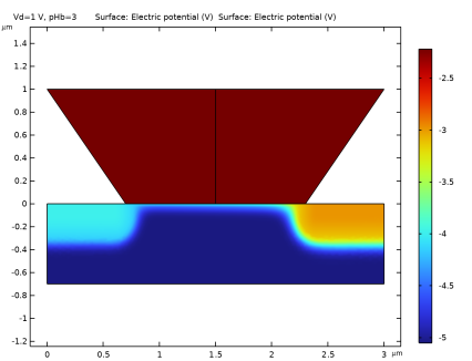
Make a colorful plot of the electric potential for the model thumbnail.
2D Plot Group 5
1
In the Results toolbar, click  2D Plot Group.
2
In the Settings window for 2D Plot Group, locate the Data section.
3
From the Dataset list, choose Sweep pH with fixed Id/Solution 6 (sol6).
4
From the Parameter value (pHb) list, choose 3.
Surface 1
Right-click 2D Plot Group 5 and choose Surface.
Surface 2
1
In the Model Builder window, right-click Surface 1 and choose Duplicate.
2
In the Settings window for Surface, locate the Expression section.
3
In the Expression text field, type V.
4
Click to expand the Quality section. From the Evaluation settings list, choose Manual.
5
From the Resolution list, choose No refinement.
6
Click to expand the Inherit Style section. From the Plot list, choose Surface 1.
7
In the 2D Plot Group 5 toolbar, click  Plot.