PDF

Density-Gradient Analysis of an InSb p-Channel FET
This tutorial analyzes the DC characteristics of an InSb p-Channel FET, using the density-gradient theory to add the effect of quantum confinement to the conventional drift–diffusion formulation, without a large increase of computational resources. The confinement effect is applied both in the quantum well channel and on the top insulator interface, which is close to the channel. The use of an anisotropic density-gradient effective mass matrix is demonstrated, as is the technique to configure a general field-dependent mobility model. The hole density profile and the Id–Vg curve obtained from the 2D model compare well with the published figures in the reference paper.
Introduction
As the semiconductor fabrication technology progresses to produce smaller and smaller devices, the effect of quantum confinement becomes more and more important. This tutorial follows the approach described in Ref. 1 to compute the hole density distribution and drain current as a function of the gate voltage of an InSb p-channel FET using the density-gradient theory (as reviewed in Ref. 2).
Model Definition
The model computes the hole density profile at pinch-off and the drain characteristics of an InSb p-channel FET, to be compared with Fig. 7 and 8 in Ref. 1. Not all simulation details are given in the paper. Nevertheless, the approach described in the paper is followed as closely as possible. When a parameter is not listed, a typical value found in the literature is used in the model: some of the material properties of InSb are taken from Ref. 3. The lead author of Ref. 1, Dr. Ancona, has also kindly verified that the Schottky barrier should be 0.4 eV and the Be delta doping is 2 nm thick with concentration 1·1019 cm3 (private communication). The section Modeling Instructions lists all the parameters used in the model.
The channel of the simulated structure is formed by a 5 nm thick InSb quantum well layer built on top of an AlInSb barrier bulk material. A 10 nm thick barrier layer is then added on top of the quantum well layer, followed by the p+ caps for the source and drain contacts. (See Fig. 6 in Ref. 1, though the gate is not recessed in this model.)
The quantum confinement effect for the quantum well layer is automatically accounted for with the default Continuous quasi-Fermi levels option for the Continuity/Heterojunction boundary condition, active at the well–barrier interfaces. In addition, quantum confinement effect for the top barrier layer boundary (the top barrier–vacuum interface) is added by selecting the Potential barrier option for the Insulation boundary condition active at those boundaries. The temperature is assumed to be 300 K. Fermi–Dirac statistics is used.
The density-gradient effective mass is anisotropic in this model. This is done by selecting the Diagonal option under the section Material Properties, Density-Gradient in the settings window for the Semiconductor Material Model domain condition.
A field dependent mobility model is employed by the reference paper. Even though it is sufficient to use the X-component of the electric field for the mobility model, given the simple geometry, we opt for the more general procedure, applicable to any arbitrary geometry. A Caughey–Thomas Mobility Model (E) subnode is added to the Semiconductor Material Model domain condition to provide the parallel component of the electric field to be used by the mobility model. The solver sequence is adjusted to achieve convergence for the resulting highly coupled system.
See the comments in the section Modeling Instructions for more detailed discussions on the model construction, meshing techniques, solution processes, and result visualization.
Results and Discussion
Figure 1 shows the drain current as a function of the gate voltage, to compare with Fig. 8 in Ref. 1. The general trend and threshold voltage compare well, with some minor differences in the magnitude of the current.
Figure 1: Drain current versus gate voltage curve.
Figure 2 plots the hole concentration profile at pinch-off, to compare with Fig. 7 in the reference paper. The overall agreement is quite good, with some small differences.
Figure 2: Hole concentration profile at pinch-off.
Figure 3 compares a line cut of the hole density profile at x = −100 nm with an approximate drift–diffusion profile, to show qualitatively the effect of quantum confinement both in the quantum well layer and at the top barrier–vacuum interface (y = 0 nm). The valence band edge and the quasi-Fermi level for the holes are also plotted. Note that this comparison is only qualitative, since the model is not re-solved using the conventional drift–diffusion formulation. As such, only the shape of the approximate drift–diffusion profile is representative of the result if the model was to be re-solved, and the absolute magnitude is not. Nevertheless the qualitative difference between the treatments with and without quantum confinement is well characterized by the difference in the shape of the hole concentration profiles: the lack of carrier pile-up at the heterojunctions and the repulsion of carriers from the top barrier–vacuum interface are both clearly indicative of quantum confinement effects.
Figure 3: Hole concentration: density-gradient (DG) versus drift–diffusion (DD), valence band edge (Ev), and quasi-Fermi level for holes (Efp).
References
1. M.G. Ancona, B.R. Bennett, and J.B. Boos, “Scaling projections for Sb-based p-channel FETs,” Solid-State Electronics, vol. 54, p. 1349, 2010.
2. M.G. Ancona, “Density-gradient theory: a macroscopic approach to quantum confinement and tunneling in semiconductor devices,” J. Comput. Electron., vol. 10, p. 65, 2011.
3. M. Levinshtein, S. Rumyantsev, and M. Shur, Handbook Series on Semiconductor Parameters, vol. 1, World Scientific, 1996, reprinted 2000.
Application Library path: Semiconductor_Module/Transistors/insb_pfet_density_gradient
Modeling Instructions
From the File menu, choose New.
New
In the New window, click  Model Wizard.
Model Wizard
1
In the Model Wizard window, click  2D.
2
In the Select Physics tree, select Semiconductor > Semiconductor (semi).
3
Click Add.
4
Click  Study.
The Semiconductor Equilibrium study step is suitable either to solve for systems known to be in thermal equilibrium, or, in this case, to provide a good initial condition for bias voltage sweeps starting from the equilibrium position.
5
In the Select Study tree, select Preset Studies for Selected Physics Interfaces > Semiconductor Equilibrium.
6
Geometry 1
The Model Wizard starts the COMSOL Desktop at the Geometry node. Use this chance to select a convenient length unit. Then enter some dimensional parameters for building the geometry.
1
In the Model Builder window, under Component 1 (comp1) click Geometry 1.
2
In the Settings window for Geometry, locate the Units section.
3
From the Length unit list, choose nm.
Global Definitions
Parameters 1: Geometry
1
In the Model Builder window, under Global Definitions click Parameters 1.
2
In the Settings window for Parameters, type Parameters 1: Geometry in the Label text field.
3
Locate the Parameters section. In the table, enter the following settings:
Geometry 1
Rectangle 1 (r1)
1
In the Geometry toolbar, click  Rectangle.
2
In the Settings window for Rectangle, locate the Size and Shape section.
3
In the Width text field, type Ltot.
4
In the Height text field, type Hstack.
5
Locate the Position section. In the x text field, type -Ltot/2.
6
In the y text field, type -Hstack.
7
Click to expand the Layers section. In the table, enter the following settings:
Rectangle 2 (r2)
1
In the Geometry toolbar, click  Rectangle.
2
In the Settings window for Rectangle, locate the Size and Shape section.
3
In the Width text field, type Ltot.
4
In the Height text field, type Hcap.
5
Locate the Position section. In the x text field, type -Ltot/2.
6
Locate the Layers section. Clear the Layers on bottom checkbox.
7
Select the Layers to the left checkbox.
8
Select the Layers to the right checkbox.
9
Delete Entities 1 (del1)
1
In the Model Builder window, right-click Geometry 1 and choose Delete Entities.
2
In the Settings window for Delete Entities, locate the Entities or Objects to Delete section.
3
From the Geometric entity level list, choose Domain.
4
On the object r2, select Domains 2 and 4 only.
Enter some material parameters and then use the built-in silicon material as a template to apply the material data. Parameters not found in the reference paper are taken from volume 1 of Handbook Series on Semiconductor Parameters edited by Levinshtein, Rumyantsev, and Shur (1996, reprinted 2000). The electron affinity of the barrier is calculated to give the value of the valence band offset given in the reference paper. Use the continuation parameter to prepare for the ramp up of the band offsets from small values in order to achieve better convergence.
Global Definitions
Parameters 2: Materials
1
In the Home toolbar, click  Parameters and choose Add > Parameters.
2
In the Settings window for Parameters, type Parameters 2: Materials in the Label text field.
3
Locate the Parameters section. In the table, enter the following settings:
Add Material
1
In the Home toolbar, click  Add Material to open the Add Material window.
2
Go to the Add Material window.
3
In the tree, select Semiconductors > Si - Silicon.
4
Click the Add to Component button in the window toolbar.
5
In the Home toolbar, click  Add Material to close the Add Material window.
Materials
InSb Well
1
In the Settings window for Material, type InSb Well in the Label text field.
2
Locate the Geometric Entity Selection section. Click  Clear Selection.
3
Create an explicit selection item for the well domain to be reused later.
4
Click  Create Selection.
5
In the Create Selection dialog, type Well domain in the Selection name text field.
6
7
In the Settings window for Material, locate the Material Contents section.
8
AlInSb Barrier
1
Right-click InSb Well and choose Duplicate.
2
In the Settings window for Material, type AlInSb Barrier in the Label text field.
3
Similarly create an explicit selection item for the barrier domains to be reused later.
4
Locate the Geometric Entity Selection section. Click  Create Selection.
5
In the Create Selection dialog, type Barrier domains in the Selection name text field.
6
7
In the Settings window for Material, locate the Material Contents section.
8
Configure physics settings. Select the density-gradient formulation from the Discretization section of the main physics settings window. Specify the anisotropic density-gradient effective mass in the settings window for the Semiconductor Material Model domain feature. Note that even though the out-of-plane component is shown and editable, its value does not affect the result, since it appears as a common factor in the numerator and denominator of the inverse matrix formula, so it cancels out to give a common factor of 1 (except when it’s zero, then zero divided by zero gives NaN, not 1). Therefore just leave its value as the default me_const.
Semiconductor (semi)
1
In the Model Builder window, under Component 1 (comp1) click Semiconductor (semi).
2
3
In the Settings window for Semiconductor, locate the Domain Selection section.
4
Click  Create Selection.
5
In the Create Selection dialog, type Semiconductor domains in the Selection name text field.
6
7
In the Settings window for Semiconductor, locate the Thickness section.
8
In the d text field, type d0.
9
Locate the Model Properties section. From the Carrier statistics list, choose Fermi–Dirac.
10
From the Solution list, choose Majority carriers only.
11
From the Majority carriers list, choose Holes.
12
Click to expand the Discretization section. From the Formulation list, choose Finite element density-gradient (quadratic shape function).
Semiconductor Material Model 1
1
In the Model Builder window, under Component 1 (comp1) > Semiconductor (semi) click Semiconductor Material Model 1.
2
In the Settings window for Semiconductor Material Model, locate the Model Input section.
3
In the T text field, type 300[K].
4
Locate the Material Properties, Density-Gradient section. From the list, choose Symmetric.
5
Specify the mhDG matrix as
For the hole mobility, select the User defined option and we will use variable definitions to implement the mobility model as specified by Eq. (3) in the reference paper. For the electric field component parallel to the local current density vector, even though it is a good enough approximation to just use the X component of the field (semi.EX), here we demonstrate how to instead use the built-in mobility model Caughey-Thomas Mobility Model (E) to obtain the parallel electric field component (semi.smm1.mmct1.Epp); an approach that is applicable to any general geometric arrangement.
6
Locate the Mobility Model section. From the μp list, choose User defined. In the associated text field, type muptot.
The variable is not yet defined, so it turns into yellow colored. Once it is defined, it will turn back to black colored. Now add the Caughey-Thomas Mobility Model (E) subnode. There is no need to enter any of the parameters, since the only purpose of this subnode is to provide the electric field component parallel to the local current density vector.
Caughey–Thomas Mobility Model (E) 1
In the Physics toolbar, click  Attributes and choose Caughey–Thomas Mobility Model (E).
Now define the mobility model variables; afterward the yellow variable should turn back to black colored. First define some physics setting parameters.
Global Definitions
Parameters 3: Physics
1
In the Home toolbar, click  Parameters and choose Add > Parameters.
2
In the Settings window for Parameters, type Parameters 3: Physics in the Label text field.
3
Locate the Parameters section. In the table, enter the following settings:
The low field mobility is different for different materials, as seen in the parameter definitions earlier. Create a common variable in each material domain(s) so that one single set of formulas for the mobility model can be shared among different materials. Use the explicit selection items defined earlier to streamline the process of selecting domains for the variable definition.
Definitions
Variables 1: Low field mobility, well
1
In the Model Builder window, under Component 1 (comp1) right-click Definitions and choose Variables.
2
In the Settings window for Variables, type Variables 1: Low field mobility, well in the Label text field.
3
Locate the Geometric Entity Selection section. From the Geometric entity level list, choose Domain.
4
From the Selection list, choose Well domain.
5
Locate the Variables section. In the table, enter the following settings:
Variables 2: Low field mobility, barrier
1
Right-click Variables 1: Low field mobility, well and choose Duplicate.
2
In the Settings window for Variables, type Variables 2: Low field mobility, barrier in the Label text field.
3
Locate the Geometric Entity Selection section. From the Selection list, choose Barrier domains.
4
Locate the Variables section. In the table, enter the following settings:
Variables 3: Mobility model
1
In the Model Builder window, right-click Definitions and choose Variables.
2
In the Settings window for Variables, type Variables 3: Mobility model in the Label text field.
3
Locate the Variables section. In the table, enter the following settings:
Add doping features with continuation parameters to prepare for the ramp up of doping concentrations from small values in order to achieve better convergence.
Semiconductor (semi)
Analytic Doping Model 1: p+ cap
1
In the Physics toolbar, click  Domains and choose Analytic Doping Model.
2
In the Settings window for Analytic Doping Model, type Analytic Doping Model 1: p+ cap in the Label text field.
3
4
Locate the Impurity section. In the NA0 text field, type NaCap*cp.
Analytic Doping Model 2: Delta doping
1
In the Physics toolbar, click  Domains and choose Analytic Doping Model.
2
In the Settings window for Analytic Doping Model, type Analytic Doping Model 2: Delta doping in the Label text field.
3
4
Locate the Distribution section. From the list, choose Box.
5
Locate the Impurity section. In the NA0 text field, type NaDelta*cp.
6
Locate the Uniform Region section. Specify the r0 vector as
7
In the W text field, type Ltot.
8
In the D text field, type 0.2*Htopbar.
9
Locate the Profile section. From the Specify profile length scale list, choose Decay length.
10
In the ld text field, type 0.02*Htopbar.
Add source, drain, and gate contacts. For the gate Schottky contact, zero out the effective Richardson constant for electrons to eliminate the possibility of unphysical electron current as a result of the majority carrier formulation for holes.
Metal Contact 1: Source
1
In the Physics toolbar, click  Boundaries and choose Metal Contact.
2
In the Settings window for Metal Contact, type Metal Contact 1: Source in the Label text field.
3
Metal Contact 2: Drain
1
In the Physics toolbar, click  Boundaries and choose Metal Contact.
2
In the Settings window for Metal Contact, type Metal Contact 2: Drain in the Label text field.
3
4
Locate the Terminal section. In the V0 text field, type Vd.
Metal Contact 3: Gate
1
In the Physics toolbar, click  Boundaries and choose Metal Contact.
2
In the Settings window for Metal Contact, type Metal Contact 3: Gate in the Label text field.
3
4
Locate the Terminal section. In the V0 text field, type Vg.
5
Locate the Contact Type section. From the Type list, choose Ideal Schottky.
6
Locate the Contact Properties section. From the Barrier height list, choose User defined. In the ΦB text field, type PhiB.
7
Locate the Thermionic Currents section. In the An text field, type 0[A/(K*cm)^2].
Add quantum confinement effect at the top barrier layer boundaries (the top barrier-vacuum interfaces). Use a large value for the barrier height to simulate the infinite barrier for holes.
Insulation 2
1
In the Physics toolbar, click  Boundaries and choose Insulation.
2
3
In the Settings window for Insulation, locate the Density-Gradient section.
4
From the Formulation list, choose Potential barrier.
5
In the ΦpOx text field, type 1000[V].
Use the Distribution feature to help create an efficient Mapped mesh that minimizes the number of mesh elements while still resolving large gradients in the solution fields.
Mesh 1
Edge 1
1
In the Mesh toolbar, click  More Generators and choose Edge.
2
Distribution 1
1
Right-click Edge 1 and choose Distribution.
2
In the Settings window for Distribution, locate the Distribution section.
3
From the Distribution type list, choose Predefined.
4
In the Number of elements text field, type 20.
5
In the Element ratio text field, type 5.
6
Select the Symmetric distribution checkbox.
Edge 2
1
In the Model Builder window, under Component 1 (comp1) > Mesh 1 right-click Edge 1 and choose Duplicate.
2
In the Settings window for Edge, locate the Boundary Selection section.
3
Click  Clear Selection.
4
Distribution 1
1
In the Model Builder window, expand the Edge 2 node, then click Distribution 1.
2
In the Settings window for Distribution, locate the Distribution section.
3
In the Number of elements text field, type 10.
4
In the Element ratio text field, type 2.5.
Edge 3
1
In the Model Builder window, under Component 1 (comp1) > Mesh 1 right-click Edge 2 and choose Duplicate.
2
In the Settings window for Edge, locate the Boundary Selection section.
3
Click  Clear Selection.
4
Distribution 1
1
In the Model Builder window, expand the Edge 3 node, then click Distribution 1.
2
In the Settings window for Distribution, locate the Distribution section.
3
In the Number of elements text field, type 12.
4
In the Element ratio text field, type 6.
5
Clear the Symmetric distribution checkbox.
Edge 4
1
In the Model Builder window, under Component 1 (comp1) > Mesh 1 right-click Edge 3 and choose Duplicate.
2
In the Settings window for Edge, locate the Boundary Selection section.
3
Click  Clear Selection.
4
Copy Edge 1
1
In the Model Builder window, right-click Mesh 1 and choose Copying Operations > Copy Edge.
2
3
In the Settings window for Copy Edge, locate the Destination Boundaries section.
4
Click to select the  Activate Selection toggle button.
5
Copy Edge 2
1
Right-click Mesh 1 and choose Copying Operations > Copy Edge.
2
3
In the Settings window for Copy Edge, locate the Destination Boundaries section.
4
Click to select the  Activate Selection toggle button.
5
Mapped 1
1
In the Mesh toolbar, click  Mapped.
2
In the Settings window for Mapped, locate the Domain Selection section.
3
From the Geometric entity level list, choose Domain.
4
From the Selection list, choose Semiconductor domains.
Distribution 1
1
Right-click Mapped 1 and choose Distribution.
2
3
In the Settings window for Distribution, locate the Distribution section.
4
From the Distribution type list, choose Predefined.
5
In the Number of elements text field, type 20.
6
In the Element ratio text field, type 5.
7
Select the Symmetric distribution checkbox.
Distribution 2
1
Right-click Distribution 1 and choose Duplicate.
2
In the Settings window for Distribution, locate the Boundary Selection section.
3
Click  Clear Selection.
4
5
Locate the Distribution section. In the Number of elements text field, type 10.
Distribution 3
1
Right-click Distribution 2 and choose Duplicate.
2
In the Settings window for Distribution, locate the Boundary Selection section.
3
Click  Clear Selection.
4
5
Locate the Distribution section. In the Element ratio text field, type 10.
6
Clear the Symmetric distribution checkbox.
Distribution 4
1
Right-click Distribution 3 and choose Duplicate.
2
In the Settings window for Distribution, locate the Boundary Selection section.
3
Click  Clear Selection.
4
5
Locate the Distribution section. In the Number of elements text field, type 25.
6
In the Element ratio text field, type 50.
7
Select the Reverse direction checkbox.
Edge 5
1
In the Mesh toolbar, click  More Generators and choose Edge.
2
3
In the Settings window for Edge, click  Build All.
Use the Auxiliary sweep feature to ramp up the doping concentrations and band offsets from small values in order to achieve better convergence. The built-in mobility model Caughey-Thomas Mobility Model (E) creates additional degrees of freedom to solve the implicit equations for the parallel electric field components. At this stage it is not necessary to solve those equations, since here we only solve for the equilibrium state to provide a good initial condition for subsequent studies. Therefore disable the mobility model node in the Modify model configuration for study step window.
Study 1: Ramp doping and band offset
1
In the Model Builder window, click Study 1.
2
In the Settings window for Study, type Study 1: Ramp doping and band offset in the Label text field.
3
Locate the Study Settings section. Clear the Generate default plots checkbox.
Step 1: Semiconductor Equilibrium
1
In the Model Builder window, under Study 1: Ramp doping and band offset click Step 1: Semiconductor Equilibrium.
2
In the Settings window for Semiconductor Equilibrium, locate the Physics and Variables Selection section.
3
Select the Modify model configuration for study step checkbox.
4
In the tree, select Component 1 (comp1) > Semiconductor (semi) > Semiconductor Material Model 1 > Caughey–Thomas Mobility Model (E) 1.
5
Click  Disable.
6
Click to expand the Study Extensions section. Select the Auxiliary sweep checkbox.
7
8
9
In the Study toolbar, click  Compute.
Add a study to sweep the drain and gate voltages, using the solution from the previous study as the initial condition. The voltages are swept from 0 (equilibrium) up to the starting point of the next study. The result of this study will be used as the initial condition for the next study, which will do a further sweep to produce the I-V curve. Set "reuse solution" to "Yes".
Add Study
1
In the Study toolbar, click  Add Study to open the Add Study window.
2
Go to the Add Study window.
3
Find the Studies subsection. In the Select Study tree, select General Studies > Stationary.
4
Click the Add Study button in the window toolbar.
5
In the Study toolbar, click  Add Study to close the Add Study window.
Study 2
Step 1: Stationary
1
In the Settings window for Stationary, click to expand the Values of Dependent Variables section.
2
Find the Initial values of variables solved for subsection. From the Settings list, choose User controlled.
3
From the Method list, choose Solution.
4
From the Study list, choose Study 1: Ramp doping and band offset, Semiconductor Equilibrium.
5
From the Parameter value (cp) list, choose Last.
6
Click to expand the Study Extensions section. Select the Auxiliary sweep checkbox.
7
8
9
10
11
12
From the Reuse solution from previous step list, choose Yes.
13
In the Model Builder window, click Study 2.
14
In the Settings window for Study, type Study 2: Ramp Vd and Vg (only as init cond for next study) in the Label text field.
15
Locate the Study Settings section. Clear the Generate default plots checkbox.
16
In the Study toolbar, click  Compute.
Add a study to sweep the gate voltage for the Id-Vg curve, using the solution from the previous study as the initial condition.
Add Study
1
In the Study toolbar, click  Add Study to open the Add Study window.
2
Go to the Add Study window.
3
Find the Studies subsection. In the Select Study tree, select General Studies > Stationary.
4
Click the Add Study button in the window toolbar.
5
In the Study toolbar, click  Add Study to close the Add Study window.
Study 3: Vg sweep for Id-Vg curve
1
In the Settings window for Stationary, locate the Values of Dependent Variables section.
2
Find the Initial values of variables solved for subsection. From the Settings list, choose User controlled.
3
From the Method list, choose Solution.
4
From the Study list, choose Study 2: Ramp Vd and Vg (only as init cond for next study), Stationary.
5
From the Parameter value (Vg (V),Vd (V)) list, choose Last.
6
Locate the Study Extensions section. Select the Auxiliary sweep checkbox.
7
From the Sweep type list, choose All combinations.
8
9
10
11
12
13
In the Model Builder window, click Study 3.
14
In the Settings window for Study, type Study 3: Vg sweep for Id-Vg curve in the Label text field.
15
In the Study toolbar, click  Compute.
Results
N-Type
The model has only p-type dopant therefore, the n-type part of the default generated plot is not needed.
1
In the Model Builder window, expand the Net Dopant Concentration (semi) node.
2
Right-click N-Type and choose Delete.
Plot the Id-Vg curve to be compared with Fig. 8 in the reference paper.
Id-Vg
1
In the Results toolbar, click  1D Plot Group.
2
In the Settings window for 1D Plot Group, type Id-Vg in the Label text field.
3
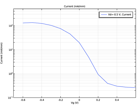
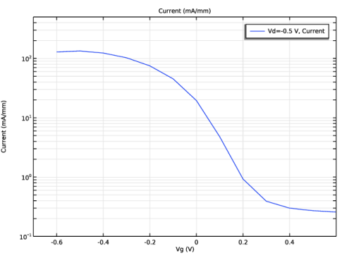
Locate the Data section. From the Dataset list, choose Study 3: Vg sweep for Id-Vg curve/Solution 3 (sol3).
4
Locate the Axis section. Select the Manual axis limits checkbox.
5
In the x minimum text field, type -0.7.
6
In the x maximum text field, type 0.6.
7
In the y minimum text field, type 0.1.
8
In the y maximum text field, type 500.
9
Select the y-axis log scale checkbox.
Global 1
1
Right-click Id-Vg and choose Global.
2
In the Settings window for Global, locate the y-Axis Data section.
3
4
In the Id-Vg toolbar, click  Plot.
Adjust the hole concentration plot to be compared with Fig. 7 in the reference paper.
Hole Concentration (semi)
1
In the Model Builder window, under Results click Hole Concentration (semi).
2
In the Settings window for 2D Plot Group, locate the Data section.
3
From the Parameter value (Vg (V)) list, choose 0.3.
Surface 1
1
In the Model Builder window, expand the Hole Concentration (semi) node, then click Surface 1.
2
In the Settings window for Surface, click to expand the Range section.
3
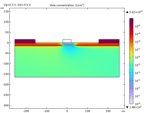
Select the Manual color range checkbox.
4
In the Minimum text field, type 10^10.
5
In the Maximum text field, type 10^21.
6
In the Hole Concentration (semi) toolbar, click  Plot.
As an example to show the quantum confinement effects introduced by the density-gradient formulation, compare the hole density profile with an approximate drift-diffusion profile on a cut line. The model is not recomputed, instead, to save time, the valence band edge and the quasi-Fermi level for the holes (both also plotted) are used in the drift-diffusion formula as is, to provide a crude approximation for the qualitative comparison. The effect of confinement in both the quantum well and the top barrier-vacuum interface (y = 0 nm) is clearly seen in the difference in the shapes of the profiles of the hole concentration.
Cut Line 2D 1
1
In the Results toolbar, click  Cut Line 2D.
2
In the Settings window for Cut Line 2D, locate the Data section.
3
From the Dataset list, choose Study 3: Vg sweep for Id-Vg curve/Solution 3 (sol3).
4
Locate the Line Data section. In row Point 1, set X to -100[nm].
5
In row Point 2, set X to -100[nm].
6
In row Point 2, set Y to -30[nm].
Hole Concentration Line Cut
1
In the Results toolbar, click  1D Plot Group.
2
In the Settings window for 1D Plot Group, type Hole Concentration Line Cut in the Label text field.
3
Locate the Data section. From the Dataset list, choose Cut Line 2D 1.
4
From the Parameter selection (Vg) list, choose From list.
5
In the Parameter values (Vg (V)) list box, select 0.3.
6
Click to expand the Title section. From the Title type list, choose Manual.
7
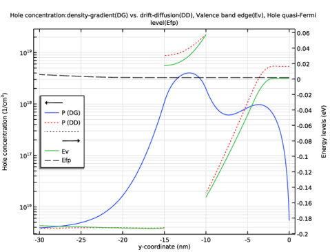
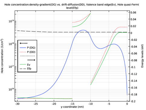
In the Title text area, type Hole concentration:density-gradient(DG) vs. drift-diffusion(DD), Valence band edge(Ev), Hole quasi-Fermi level(Efp).
8
Locate the Plot Settings section. Select the Two y-axes checkbox.
9
Select the Secondary y-axis label checkbox. In the associated text field, type Energy levels (eV).
10
Locate the Legend section. From the Position list, choose Middle left.
Line Graph 1
1
Right-click Hole Concentration Line Cut and choose Line Graph.
2
In the Settings window for Line Graph, locate the y-Axis Data section.
3
In the Expression text field, type semi.P.
4
In the Unit field, type 1/cm^3.
5
Locate the x-Axis Data section. From the Parameter list, choose Expression.
6
In the Expression text field, type y.
7
Click to expand the Legends section. Select the Show legends checkbox.
8
From the Legends list, choose Manual.
9
Line Graph 2
1
Right-click Line Graph 1 and choose Duplicate.
2
In the Settings window for Line Graph, locate the y-Axis Data section.
3
In the Expression text field, type semi.Nv*semi.FD_half((semi.Ev-semi.Efp)/semi.Vth).
4
Select the Description checkbox. In the associated text field, type Hole concentration.
5
Click to expand the Coloring and Style section. Find the Line style subsection. From the Line list, choose Dotted.
6
From the Color list, choose Red.
7
Locate the Legends section. In the table, enter the following settings:
Line Graph 3
1
Right-click Line Graph 2 and choose Duplicate.
2
In the Settings window for Line Graph, locate the y-Axis section.
3
Select the Plot on secondary y-axis checkbox.
4
Locate the y-Axis Data section. In the Expression text field, type semi.Ev.
5
Locate the Legends section. In the table, enter the following settings:
6
Locate the y-Axis Data section. Clear the Description checkbox.
7
Locate the Coloring and Style section. Find the Line style subsection. From the Line list, choose Solid.
8
From the Color list, choose Cycle.
Line Graph 4
1
Right-click Line Graph 3 and choose Duplicate.
2
In the Settings window for Line Graph, locate the y-Axis Data section.
3
In the Expression text field, type semi.Efp.
4
Locate the Coloring and Style section. Find the Line style subsection. From the Line list, choose Dashed.
5
From the Color list, choose Black.
6
Locate the Legends section. In the table, enter the following settings:
7
Click the  y-Axis Log Scale button in the Graphics toolbar.
8
In the Hole Concentration Line Cut toolbar, click  Plot.