|
|
|
|
|
|
1
|
In the Model Wizard window, The model is 1D in nature. However to demonstrate the general procedure for setting up 2D and 3D models, we will build an equivalent 2D model.
|
|
2
|
click
|
|
3
|
|
4
|
Click Add.
|
|
5
|
|
6
|
Click Add.
|
|
7
|
Click Add.
|
|
8
|
Click
|
|
9
|
|
10
|
Click
|
|
1
|
|
2
|
|
3
|
|
1
|
|
2
|
|
3
|
Click
|
|
4
|
Browse to the model’s Application Libraries folder and double-click the file heterojunction_tunneling_parameters.txt.
|
|
1
|
|
2
|
|
3
|
|
4
|
|
5
|
|
6
|
|
7
|
Select the Layers to the left checkbox.
|
|
9
|
Click
|
|
1
|
In the Model Builder window, under Component 1 (comp1) right-click Definitions and choose Variables.
|
|
2
|
|
3
|
|
5
|
Locate the Variables section. In the table, enter the following settings:
|
|
1
|
|
2
|
|
4
|
Locate the Variables section. In the table, enter the following settings:
|
|
1
|
|
2
|
|
4
|
Locate the Variables section. In the table, enter the following settings:
|
|
1
|
In the Model Builder window, under Component 1 (comp1) right-click Materials and choose Blank Material.
|
|
2
|
|
3
|
In the Model Builder window, expand the Component 1 (comp1) > Materials > Al(x)Ga(1-x)As (Yang et al 1993) (mat1) node, then click Basic (def).
|
|
4
|
|
5
|
In the Local properties table, enter the following settings:
|
|
6
|
In the Model Builder window, under Component 1 (comp1) > Materials click Al(x)Ga(1-x)As (Yang et al 1993) (mat1).
|
|
7
|
|
1
|
|
1
|
|
1
|
|
1
|
|
1
|
|
1
|
|
1
|
In the Model Builder window, under Component 1 (comp1) right-click Definitions and choose Variables.
|
|
2
|
|
3
|
|
5
|
Locate the Variables section. In the table, enter the following settings:
|
|
1
|
|
2
|
|
3
|
|
4
|
Click to expand the Discretization section. From the Formulation list, choose Finite element quasi Fermi level (quadratic shape function).
|
|
5
|
|
6
|
In the Show More Options dialog, in the tree, select the checkbox for the node Physics > Advanced Physics Options.
|
|
7
|
Click OK.
|
|
8
|
|
9
|
|
1
|
In the Model Builder window, under Component 1 (comp1) > Semiconductor (semi) click Semiconductor Material Model 1.
|
|
2
|
|
3
|
|
4
|
Click to expand the Dopant Ionization section. From the Dopant ionization list, choose Incomplete ionization.
|
|
5
|
|
6
|
|
1
|
|
2
|
|
3
|
|
1
|
Right-click Component 1 (comp1) > Semiconductor (semi) > Continuity/Heterojunction 1 and choose Duplicate.
|
|
2
|
|
3
|
Click
|
|
5
|
Click to expand the Extra Current Contribution section. From the Extra electron current list, choose WKB tunneling model.
|
|
1
|
|
2
|
In the Settings window for WKB Tunneling Model, Electrons, locate the Potential Barrier Domain Selection section.
|
|
3
|
Click to select the
|
|
5
|
Locate the Opposite Boundary Selection section. Click to select the
|
|
7
|
|
8
|
|
9
|
|
1
|
|
2
|
|
3
|
|
4
|
|
5
|
|
1
|
|
2
|
|
3
|
|
1
|
In the Model Builder window, under Component 1 (comp1) > Materials click Al(x)Ga(1-x)As (Yang et al 1993) (mat1).
|
|
2
|
|
1
|
|
3
|
|
4
|
|
1
|
|
1
|
|
1
|
|
2
|
|
1
|
|
2
|
|
3
|
In the Solve for column of the table, under Component 1 (comp1), clear the checkboxes for Curvilinear Coordinates (cc) and Curvilinear Coordinates 2 (cc2).
|
|
4
|
Select the Modify model configuration for study step checkbox.
|
|
5
|
|
6
|
Click
|
|
7
|
|
8
|
Click
|
|
10
|
|
1
|
|
2
|
|
1
|
|
2
|
|
3
|
|
4
|
|
5
|
Locate the Plot Settings section.
|
|
6
|
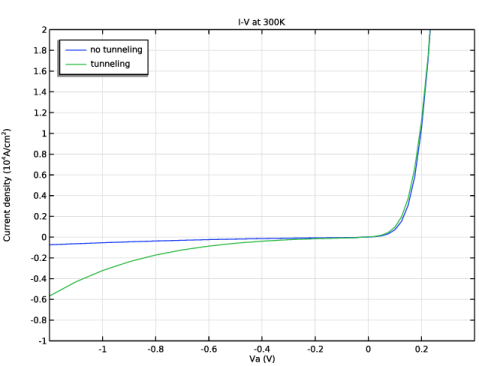
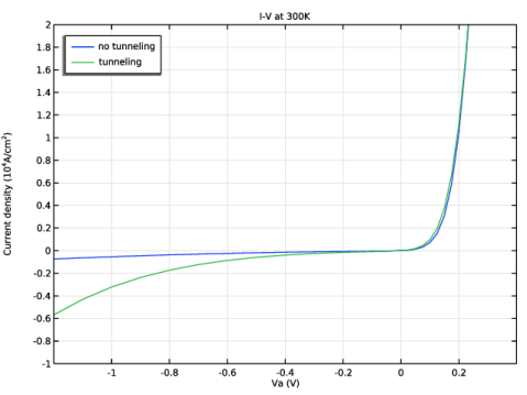
Select the y-axis label checkbox. In the associated text field, type Current density (10<sup>4</sup>A/cm<sup>2</sup>).
|
|
7
|
|
8
|
|
9
|
|
10
|
|
11
|
|
1
|
|
2
|
|
4
|
|
1
|
|
2
|
Go to the Add Study window.
|
|
3
|
Find the Physics interfaces in study subsection. In the table, clear the Solve checkbox for Semiconductor (semi).
|
|
4
|
|
5
|
Click the Add Study button in the window toolbar.
|
|
6
|
|
1
|
|
2
|
|
1
|
|
2
|
|
3
|
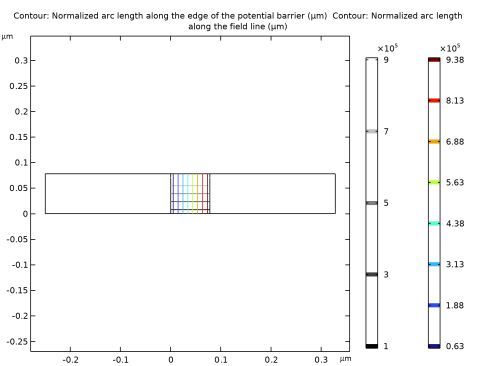
Locate the Data section. From the Dataset list, choose Study 2: curvilinear coordinates/Solution 2 (sol2).
|
|
1
|
|
2
|
|
3
|
|
4
|
|
1
|
|
2
|
|
3
|
|
4
|
|
1
|
|
2
|
|
3
|
|
4
|
|
1
|
|
2
|
Go to the Add Study window.
|
|
3
|
Find the Physics interfaces in study subsection. In the table, clear the Solve checkboxes for Curvilinear Coordinates (cc) and Curvilinear Coordinates 2 (cc2).
|
|
4
|
|
5
|
Click the Add Study button in the window toolbar.
|
|
6
|
|
1
|
|
2
|
|
3
|
Find the Initial values of variables solved for subsection. From the Settings list, choose User controlled.
|
|
4
|
|
5
|
|
6
|
|
7
|
Find the Values of variables not solved for subsection. From the Settings list, choose User controlled.
|
|
8
|
|
9
|
|
10
|
|
11
|
Click
|
|
13
|
|
1
|
In the Model Builder window, under Results > I-V at 300 K right-click Global 1 and choose Duplicate.
|
|
2
|
|
3
|
|
4
|
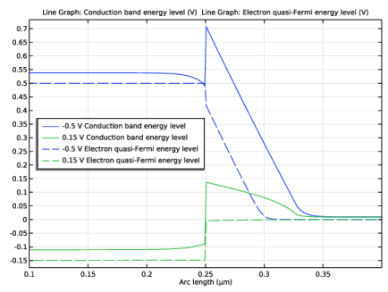
Locate the y-Axis Data section. In the table, enter the following settings:
|
|
5
|
|
1
|
|
2
|
|
3
|
|
4
|
|
5
|
|
1
|
|
3
|
|
4
|
|
5
|
|
6
|
|
7
|
|
8
|
|
1
|
|
2
|
|
3
|
|
4
|
Click to expand the Coloring and Style section. Find the Line style subsection. From the Line list, choose Dashed.
|
|
5
|
|
1
|
|
2
|
|
3
|
Select the Manual axis limits checkbox.
|
|
4
|
|
5
|
|
6
|
|
7
|
|
1
|
|
2
|
Go to the Add Study window.
|
|
3
|
|
4
|
Click the Add Study button in the window toolbar.
|
|
5
|
|
1
|
|
3
|
Click to expand the Values of Dependent Variables section. Find the Initial values of variables solved for subsection. From the Settings list, choose User controlled.
|
|
4
|
|
5
|
|
6
|
|
1
|
|
2
|
|
3
|
Click
|
|
5
|
Click
|
|
7
|
|
1
|
|
2
|
|
1
|
|
2
|
|
4
|
|
5
|
|
6
|
Click to expand the Coloring and Style section. Find the Line style subsection. From the Line list, choose Dotted.
|
|
1
|
|
2
|
|
3
|
|
4
|
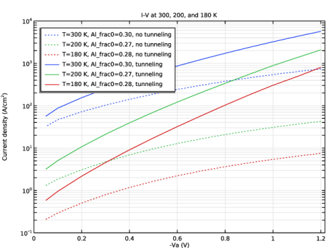
In the Parameter values (Va (V)) list, choose -1.2, -1.1, -1, -0.9, -0.8, -0.7, -0.6, -0.5, -0.4, -0.3, -0.2, -0.1, and -0.05.
|
|
5
|
|
6
|
|
7
|
Locate the Plot Settings section.
|
|
8
|
Select the y-axis label checkbox. In the associated text field, type Current density (A/cm<sup>2</sup>).
|
|
1
|
In the Model Builder window, under Results > I-V at different Ts right-click Global 1 and choose Duplicate.
|
|
2
|
|
3
|
|
4
|
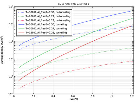
Locate the y-Axis Data section. In the table, enter the following settings:
|
|
5
|
|
6
|
|
1
|
|
2
|
Go to the Add Study window.
|
|
3
|
|
4
|
Click the Add Study button in the window toolbar.
|
|
5
|
|
1
|
|
2
|
Clear the Modify model configuration for study step checkbox.
|
|
3
|
Locate the Values of Dependent Variables section. Find the Initial values of variables solved for subsection. From the Study list, choose Study 4: no tunneling, lower Ts, Stationary.
|
|
4
|
|
5
|
|
6
|
|
7
|
Find the Values of variables not solved for subsection. From the Settings list, choose User controlled.
|
|
8
|
|
9
|
|
10
|
|
1
|
In the Model Builder window, under Results > I-V at different Ts right-click Global 1 and choose Duplicate.
|
|
2
|
|
3
|
|
4
|
|
5
|
In the Parameter values (Va (V)) list, choose -1.2, -1.1, -1, -0.9, -0.8, -0.7, -0.6, -0.5, -0.4, -0.3, -0.2, -0.1, and -0.05.
|
|
6
|
Locate the y-Axis Data section. In the table, enter the following settings:
|
|
7
|
Locate the Coloring and Style section. Find the Line style subsection. From the Line list, choose Solid.
|
|
8
|
|
1
|
|
2
|
|
3
|
|
4
|
Locate the y-Axis Data section. In the table, enter the following settings:
|
|
5
|
|
1
|
|
2
|
|
3
|
Select the Manual axis limits checkbox.
|
|
4
|
|
5
|
|
6
|
|
7
|
|
8
|