PDF

Caughey–Thomas Mobility
This example demonstrates how to use the Caughey–Thomas high-field saturation model for the electron and hole mobility. Field-dependent mobility makes a problem which is already highly nonlinear even more nonlinear. The Semiconductor physics interface automatically creates a suggested solver sequence for better convergence when a built-in field-dependent mobility model is used.
Introduction
With an increase in the parallel component of the applied field, carriers can gain energies above the ambient thermal energy and then transfer energy gained from the field to the lattice by optical phonon emission. This effect leads to a saturation of the carriers velocity.
The Caughey–Thomas mobility model adds high field velocity saturation to an existing mobility model (or to a constant input mobility), based on equations presented in Ref. 1.
The electron (μn,ct) and hole (μp,ct) mobilities are determined by the following equations:
Here T is the lattice temperature, μin,n and μin,p are the electron and hole input mobilities, respectively, and Fn and Fp are the driving forces for electrons and holes, respectively (several options are available, the default is Fn = E||,n and Fp = E||,p, where E||,n is the magnitude of the component of the electric field parallel to the electron current and E||,p is the magnitude of the component of the electric field parallel to the hole current). All other parameters in the model are material properties (note that v0,n and v0,p are the saturation velocities for electrons and holes at the reference temperature Tref and have units of m/s). The material properties for Silicon are also obtained from Ref. 1.
Model Definition
The model represents a simplified channel region of a 2D MOSFET, where the n-doped drain and source are located on the left and right side of the geometry, respectively; see Figure 1. The gate is positioned on top of the p-doped silicon section, which is located at the center of the device.
The model consists of sweeping the drain to source voltage form 0 V to 1 V under a gate to source voltage of 0 V. Sweeping the drain voltage creates a significant electric field at the left side of the gate at the p–n junction.
Figure 1: Schematic of the modeled device.
The field-dependent mobility models are very nonlinear and difficult to solve in a fully coupled manner. The Semiconductor physics interface automatically creates a suggested solver sequence when the built-in field-dependent mobility models are used. This suggested solver sequence alternately solves the main dependent variables with the electric field variables fixed and then updates the electric field variables afterward, using the Segregated solver. By default, 3 iterations are used; however, depending on the model, more iterations may be needed. For this model, 4 iterations are used for better accuracy.
Results and Discussion
Figure 2 shows the effect of the Caughey–Thomas mobility model on the solution. The comparison of the constant mobility (the driving forces Fn and Fp are multiplied by 0) and the Caughey–Thomas mobility model (Fn and Fp multiplied by 1) shows a more pronounced saturation effect for the Caughey–Thomas model.
Figure 3 shows that the electron mobility varies substantially along the device. The electron mobility is 3 order of magnitude lower in the vicinity of the drain–gate junction as a consequence of the high electric field generated by the applied potential on the drain contact.
Figure 4 and Figure 5 show the effect of the mobility model on the electron drift velocity. Figure 4 shows the electron drift velocity for the Caughey–Thomas mobility model (Fn and Fp multiplied by 1) and Figure 5 for the constant mobility model (Fn and Fp multiplied by 0). A comparison of the two figures clearly shows an important reduction of the electron drift velocity when the field effect is taken into account.
Figure 2: Comparison of the terminal current for the constant mobility and Caughey–Thomas mobility. The current is lower and levels off more rapidly due to the fact that the mobility decreases when the electric field is high.
Figure 3: Plot of the electron mobility at a drain–source voltage of 1 V. The mobility varies by 3 orders of magnitude over the modeling domain.
Figure 4: Plot of the electron drift velocity using Caughey–Thomas mobility. The drift velocity barely exceeds 1 x 105 m/s.
Figure 5: Plot of the electron drift velocity for the constant mobility case. Since the mobility does not decrease as the electric field increases, the drift velocity becomes very high.
Reference
1. C. Canali and others, “Electron and Hole Drift Velocity Measurements in Silicon and Their Empirical Relation to Electric Field and Temperature,” IEEE Transactions on Electron Devices, vol. 22, no. 11, pp. 1045–1047, 1975.
Note: Note the correction in: G. Ottaviani, “Correction to ‘Electron and Hole Drift Velocity Measurements in Silicon and Their Empirical Relation to Electric Field and Temperature’,” IEEE Transactions on Electron Devices, vol. 23, no. 9, p. 1113, 1976.
Application Library path: Semiconductor_Module/Transistors/caughey_thomas_mobility
Modeling Instructions
From the File menu, choose New.
New
In the New window, click  Model Wizard.
Model Wizard
1
In the Model Wizard window, click  2D.
2
In the Select Physics tree, select Semiconductor > Semiconductor (semi).
3
Click Add.
4
Click  Study.
5
In the Select Study tree, select General Studies > Stationary.
6
Enter model parameters.
Global Definitions
Parameters 1
1
In the Model Builder window, under Global Definitions click Parameters 1.
2
In the Settings window for Parameters, locate the Parameters section.
3
Create model geometry representing a simplified channel region of a field effect transistor.
Geometry 1
1
In the Model Builder window, under Component 1 (comp1) click Geometry 1.
2
In the Settings window for Geometry, locate the Units section.
3
From the Length unit list, choose nm.
Rectangle 1 (r1)
1
In the Geometry toolbar, click  Rectangle.
2
In the Settings window for Rectangle, locate the Size and Shape section.
3
In the Width text field, type Lg.
4
In the Height text field, type Wfin/2.
Rectangle 2 (r2)
1
In the Geometry toolbar, click  Rectangle.
2
In the Settings window for Rectangle, locate the Size and Shape section.
3
In the Height text field, type Wfin/2.
4
Locate the Position section. In the x text field, type -1.
Rectangle 3 (r3)
1
In the Geometry toolbar, click  Rectangle.
2
In the Settings window for Rectangle, locate the Size and Shape section.
3
In the Height text field, type Wfin/2.
4
Locate the Position section. In the x text field, type Lg.
5
Click  Build All Objects.
Add the built-in silicon material properties.
Add Material
1
In the Materials toolbar, click  Add Material to open the Add Material window.
2
Go to the Add Material window.
3
In the tree, select Semiconductors > Si - Silicon.
4
Click the Add to Component button in the window toolbar.
5
In the Materials toolbar, click  Add Material to close the Add Material window.
Enter physics settings.
Semiconductor (semi)
1
In the Settings window for Semiconductor, click to expand the Continuation Settings section.
2
In the Cp text field, type ds.
Analytic Doping Model 1
1
In the Physics toolbar, click  Domains and choose Analytic Doping Model.
2
3
In the Settings window for Analytic Doping Model, locate the Impurity section.
4
From the Impurity type list, choose Donor doping (n-type).
5
In the ND0 text field, type 1e19[1/cm^3].
Analytic Doping Model 2
1
In the Physics toolbar, click  Domains and choose Analytic Doping Model.
2
3
In the Settings window for Analytic Doping Model, locate the Impurity section.
4
In the NA0 text field, type 1e15[1/cm^3].
Metal Contact 1
1
In the Physics toolbar, click  Boundaries and choose Metal Contact.
2
3
In the Settings window for Metal Contact, locate the Terminal section.
4
In the V0 text field, type Vds.
Metal Contact 2
1
In the Physics toolbar, click  Boundaries and choose Metal Contact.
2
Thin Insulator Gate 1
1
In the Physics toolbar, click  Boundaries and choose Thin Insulator Gate.
2
3
In the Settings window for Thin Insulator Gate, locate the Terminal section.
4
In the V0 text field, type Vgs.
5
Locate the Gate Contact section. In the εins text field, type 3.9.
6
In the dins text field, type tox.
Semiconductor Material Model 1
In the Model Builder window, click Semiconductor Material Model 1.
Caughey–Thomas Mobility Model (E) 1
1
In the Physics toolbar, click  Attributes and choose Caughey–Thomas Mobility Model (E).
2
In the Settings window for Caughey–Thomas Mobility Model (E), click to expand the Continuation Settings section.
3
From the Continuation type list, choose Use interface continuation parameter.
Do not forget to select the mobility model in the Semiconductor Material Model node, otherwise the mobility model subnode has no effect.
Semiconductor Material Model 1
1
In the Model Builder window, click Semiconductor Material Model 1.
2
In the Settings window for Semiconductor Material Model, locate the Mobility Model section.
3
From the μn list, choose Electron mobility, Caughey–Thomas (semi/smm1/mmct1).
4
From the μp list, choose Hole mobility, Caughey–Thomas (semi/smm1/mmct1).
Optionally use the finite element log formulation to compute this model.
5
In the Model Builder window, click Semiconductor (semi).
6
In the Settings window for Semiconductor, click to expand the Discretization section.
7
From the Formulation list, choose Finite element, log formulation (linear shape function).
Set up a user-defined mesh.
Mesh 1
Mapped 1
1
In the Mesh toolbar, click  Mapped.
2
In the Settings window for Mapped, click to expand the Reduce Element Skewness section.
3
Select the Adjust edge mesh checkbox.
Distribution 1
1
Right-click Mapped 1 and choose Distribution.
2
3
In the Settings window for Distribution, locate the Distribution section.
4
From the Distribution type list, choose Predefined.
5
In the Number of elements text field, type 20.
6
In the Element ratio text field, type 5.
7
From the Growth rate list, choose Exponential.
8
Select the Reverse direction checkbox.
Distribution 2
1
In the Model Builder window, right-click Mapped 1 and choose Distribution.
2
Distribution 3
1
Right-click Mapped 1 and choose Distribution.
2
3
In the Settings window for Distribution, locate the Distribution section.
4
From the Distribution type list, choose Predefined.
5
In the Number of elements text field, type 50.
6
In the Element ratio text field, type 25.
7
From the Growth rate list, choose Exponential.
8
Select the Symmetric distribution checkbox.
Set up an auxiliary sweep for the ds parameter, with the value 0 for constant mobility and 1 for mobility model.
Study 1
Step 1: Stationary
1
In the Model Builder window, under Study 1 click Step 1: Stationary.
2
In the Settings window for Stationary, click to expand the Study Extensions section.
3
Select the Auxiliary sweep checkbox.
4
5
6
7
8
From the Sweep type list, choose All combinations.
9
From the Reuse solution from previous step list, choose Auto.
The field-dependent mobility models are very nonlinear and difficult to solve in a fully coupled manner. The Semiconductor interface automatically creates a suggested solver sequence when the built-in field-dependent mobility models are used. This suggested solver sequence alternately solves the main dependent variables with the electric field variables fixed and then updates the electric field variables afterward, using the Segregated solver. By default 3 iterations are used, however depending on the model, more iterations may be needed. For this model we will use 4 iterations for better accuracy.
Solution 1 (sol1)
1
In the Study toolbar, click  Show Default Solver.
2
In the Model Builder window, expand the Solution 1 (sol1) node.
3
In the Model Builder window, expand the Study 1 > Solver Configurations > Solution 1 (sol1) > Stationary Solver 1 node, then click Segregated 1.
4
In the Settings window for Segregated, locate the General section.
5
In the Number of iterations text field, type 4.
6
In the Study toolbar, click  Compute.
Results
Electron Concentration (semi)
Click the  Zoom Extents button in the Graphics toolbar.
Terminal current_constant vs. Caughey–Thomas mobility
1
In the Results toolbar, click  1D Plot Group.
2
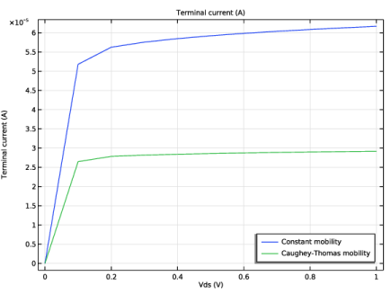
In the Settings window for 1D Plot Group, type Terminal current_constant vs. Caughey-Thomas mobility in the Label text field.
Global 1
1
Right-click Terminal current_constant vs. Caughey–Thomas mobility and choose Global.
2
In the Settings window for Global, click Replace Expression in the upper-right corner of the y-Axis Data section. From the menu, choose Component 1 (comp1) > Semiconductor > Terminals > semi.I0_1 - Terminal current - A.
3
Locate the x-Axis Data section. From the Axis source data list, choose Vds.
4
In the Terminal current_constant vs. Caughey–Thomas mobility toolbar, click  Plot.
5
Click to expand the Legends section. From the Legends list, choose Manual.
6
7
In the Terminal current_constant vs. Caughey–Thomas mobility toolbar, click  Plot.
8
Click the  Zoom Extents button in the Graphics toolbar.
Terminal current_constant vs. Caughey–Thomas mobility
1
In the Model Builder window, click Terminal current_constant vs. Caughey–Thomas mobility.
2
In the Settings window for 1D Plot Group, locate the Legend section.
3
From the Position list, choose Lower right.
Electron mobility
1
In the Results toolbar, click  2D Plot Group.
2
In the Settings window for 2D Plot Group, type Electron mobility in the Label text field.
Surface 1
1
Right-click Electron mobility and choose Surface.
2
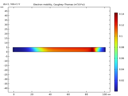
In the Settings window for Surface, click Replace Expression in the upper-right corner of the Expression section. From the menu, choose Component 1 (comp1) > Semiconductor > Mobility > semi.mun_ct - Electron mobility, Caughey–Thomas - m²/(V·s).
3
In the Electron mobility toolbar, click  Plot.
4
Click the  Zoom Extents button in the Graphics toolbar.
Electron drift velocity
1
In the Model Builder window, right-click Electron mobility and choose Duplicate.
2
In the Settings window for 2D Plot Group, type Electron drift velocity in the Label text field.
Surface 1
1
In the Model Builder window, expand the Electron drift velocity node, then click Surface 1.
2
In the Settings window for Surface, locate the Expression section.
3
In the Expression text field, type semi.mun_ct*semi.smm1.mmct1.Fn.
4
Select the Description checkbox. In the associated text field, type Electron drift velocity.
5
In the Electron drift velocity toolbar, click  Plot.
6
Click the  Zoom Extents button in the Graphics toolbar.
Electron drift velocity
1
In the Model Builder window, click Electron drift velocity.
2
In the Settings window for 2D Plot Group, locate the Data section.
3
From the Parameter value (ds) list, choose 0.
4
In the Electron drift velocity toolbar, click  Plot.
5
Click the  Zoom Extents button in the Graphics toolbar.