PDFpcb_microwave_filter_with_stress.java

Microwave Filter on PCB with Stress
Introduction
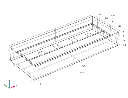
Microstrip filters can be fabricated directly on a printed circuit board (PCB) with a microstrip line going from the input to the output. Along the microstrip line there are a number of stubs of certain lengths and widths. The design of the filter involves choosing the impedance of the microstrip line, the impedance of the stub microstrips, and the stub lengths. This particular filter is based on a textbook example from Ref. 2. It is also used as example in Ref. 1, which contains results from other simulation tools and methods and is freely available online. The filter has a seven-pole low-pass Chebyshev response with a cutoff frequency of 1 GHz.
Model Definition
The model uses the Electromagnetic Waves interface that solves the vector Helmholtz wave equation. The cutoff frequency of the filter is 1 GHz by design, and the dielectric layer of the PCB has a relative permittivity of 10.8. The metal layers are modeled as perfect electric conductors with zero thickness, thereby avoiding a dense meshing of thin conductive layers. The width of the microstrip line is 0.1 mm and the width of the stubs is 5 mm.
The characteristics of the filter are sensitive to the placement and length of the stubs; therefore this example also analyzes the change in filter characteristics as a function of mechanical deformation. This is done by adding Solid Mechanics and Moving Mesh interfaces. The Moving Mesh interface is necessary to enable the Electromagnetic Waves interface to account for the deformation of the PCB. The deformation comes from a uniform load across the board with fixed input and output faces.
Because the filter cutoff should be close to 1 GHz, the frequency is swept from 750 MHz up to 1.5 GHz. The first solution step performs this sweep for the Electromagnetic Waves interface without any mechanical deformation. Then a uniform load of 40 N is applied to the PCB, generating a large deformation of the board. The Solid Mechanics interface calculates the deformation, and the Moving Mesh interface applies this deformation to the coordinate system that the Electromagnetic Waves interface uses. After this step, the frequency sweep is performed again for the Electromagnetic Waves interface using the parametric solver.
This example accounts for the structural deformation in the sense that it solves for the electromagnetic fields on the deformed geometry, as if the PCB was manufactured in the deformed shape, free of stress.
Results and Discussion
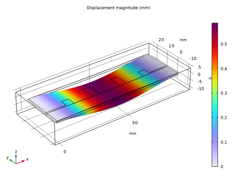
The purpose of this simulation is to analyze how the S-parameter curve changes when a force of 40 N is applied on the circuit board. This force bends the PCB significantly, as you can see in Figure 1.
Figure 1: The graph shows the total displacement of the PCB, due to the load.
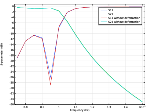
Although the PCB deformation is fairly large the S-parameter curve does not change that much. The cutoff frequency is shifted less than 10 MHz when the force is applied. Figure 2 displays the difference between the S-parameter curves with and without an applied force.
Figure 2: A comparison between the S11 and S21 parameters before and after a force of 40 N has been applied on the PCB. The red and turquoise lines correspond to the S-parameter curves for the filter with an applied force.
References
1. D.V. Tosic and M. Potrebic, “Software Tools for Research and Education,” Microwave Review, vol. 12, no. 2, pp. 45–54, 2006.
2. J.-S.G. Hong and M.J. Lancaster, Microstrip Filters for RF/Microwave Applications, John Wiley & Sons, 2001.
Application Library path: RF_Module/Filters/pcb_microwave_filter_with_stress
Modeling Instructions
From the File menu, choose New.
New
In the New window, click  Model Wizard.
Model Wizard
1
In the Model Wizard window, click  3D.
2
In the Select Physics tree, select Radio Frequency > Electromagnetic Waves, Frequency Domain (emw).
3
Click Add.
4
Click  Study.
5
In the Select Study tree, select General Studies > Frequency Domain.
6
Global Definitions
The following steps define the parameters for the frequency sweep.
Parameters 1
1
In the Model Builder window, under Global Definitions click Parameters 1.
2
In the Settings window for Parameters, locate the Parameters section.
3
Geometry 1
Set mm as the default unit for length.
1
In the Model Builder window, under Component 1 (comp1) click Geometry 1.
2
In the Settings window for Geometry, locate the Units section.
3
From the Length unit list, choose mm.
Block 1 (blk1)
1
In the Geometry toolbar, click  Block.
2
In the Settings window for Block, locate the Size and Shape section.
3
In the Width text field, type 89.49.
4
In the Depth text field, type 29.54.
5
In the Height text field, type 1.27.
6
Locate the Position section. In the y text field, type -10.
7
Click  Build Selected.
8
Click the  Wireframe Rendering button in the Graphics toolbar.
Work Plane 1 (wp1)
1
In the Geometry toolbar, click  Work Plane.
2
In the Settings window for Work Plane, locate the Plane Definition section.
3
In the z-coordinate text field, type 1.27.
Work Plane 1 (wp1) > Plane Geometry
In the Model Builder window, click Plane Geometry.
Work Plane 1 (wp1) > Rectangle 1 (r1)
1
In the Work Plane toolbar, click  Rectangle.
2
In the Settings window for Rectangle, locate the Size and Shape section.
3
In the Width text field, type 13.88.
4
In the Height text field, type 1.125.
Work Plane 1 (wp1) > Rectangle 2 (r2)
1
In the Work Plane toolbar, click  Rectangle.
2
In the Settings window for Rectangle, locate the Size and Shape section.
3
In the Width text field, type 5.
4
In the Height text field, type 5.86.
5
Locate the Position section. In the xw text field, type 13.88.
Work Plane 1 (wp1) > Rectangle 3 (r3)
1
In the Work Plane toolbar, click  Rectangle.
2
In the Settings window for Rectangle, locate the Size and Shape section.
3
In the Width text field, type 13.32.
4
In the Height text field, type 0.1.
5
Locate the Position section. In the xw text field, type 18.88.
Work Plane 1 (wp1) > Rectangle 4 (r4)
1
In the Work Plane toolbar, click  Rectangle.
2
In the Settings window for Rectangle, locate the Size and Shape section.
3
In the Width text field, type 5.
4
In the Height text field, type 9.54.
5
Locate the Position section. In the xw text field, type 32.2.
Work Plane 1 (wp1) > Rectangle 5 (r5)
1
In the Work Plane toolbar, click  Rectangle.
2
In the Settings window for Rectangle, locate the Size and Shape section.
3
In the Width text field, type 15.09.
4
In the Height text field, type 0.1.
5
Locate the Position section. In the xw text field, type 37.2.
Work Plane 1 (wp1) > Mirror 1 (mir1)
1
In the Work Plane toolbar, click  Transforms and choose Mirror.
2
Select the objects r1, r2, r3, and r4 only.
3
In the Settings window for Mirror, locate the Input section.
4
Select the Keep input objects checkbox.
5
Locate the Point on Line of Reflection section. In the xw text field, type 44.745.
Work Plane 1 (wp1) > Union 1 (uni1)
1
In the Work Plane toolbar, click  Booleans and Partitions and choose Union.
2
Click in the Graphics window and then press Ctrl+A to select all objects.
3
In the Settings window for Union, locate the Union section.
4
Clear the Keep interior boundaries checkbox.
5
Click  Build Selected.
Work Plane 2 (wp2)
1
In the Model Builder window, right-click Geometry 1 and choose Work Plane.
2
In the Settings window for Work Plane, locate the Plane Definition section.
3
In the z-coordinate text field, type 1.27.
Work Plane 2 (wp2) > Plane Geometry
In the Model Builder window, click Plane Geometry.
Work Plane 2 (wp2) > Line Segment 1 (ls1)
1
In the Work Plane toolbar, click  More Primitives and choose Line Segment.
2
In the Settings window for Line Segment, locate the Starting Point section.
3
From the Specify list, choose Coordinates.
4
Locate the Endpoint section. From the Specify list, choose Coordinates.
5
In the yw text field, type 1.125.
Work Plane 2 (wp2) > Mirror 1 (mir1)
1
In the Work Plane toolbar, click  Transforms and choose Mirror.
2
3
In the Settings window for Mirror, locate the Input section.
4
Select the Keep input objects checkbox.
5
Locate the Point on Line of Reflection section. In the xw text field, type 44.745.
6
Click  Build Selected.
The next step is to add boundary faces for the input and output ports by extruding the lines.
Extrude 1 (ext1)
1
In the Model Builder window, right-click Geometry 1 and choose Extrude.
2
In the Settings window for Extrude, locate the Distances section.
3
Block 2 (blk2)
1
In the Geometry toolbar, click  Block.
2
In the Settings window for Block, locate the Size and Shape section.
3
In the Width text field, type 100.
4
In the Depth text field, type 40.
5
In the Height text field, type 15.
6
Locate the Position section. In the x text field, type -5.
7
In the y text field, type -15.
8
In the z text field, type -10.
9
In the Geometry toolbar, click  Build All.
Disable the analysis of the geometry as the remaining small geometric details are needed.
10
In the Model Builder window, click Geometry 1.
11
In the Settings window for Geometry, locate the Cleanup section.
12
Clear the Automatic detection of small details checkbox.
Add Material
1
In the Materials toolbar, click  Add Material to open the Add Material window.
2
Go to the Add Material window.
3
In the tree, select Built-in > Air.
4
Click the Add to Component button in the window toolbar.
5
In the tree, select Built-in > FR4 (Circuit Board).
6
Click the Add to Component button in the window toolbar.
7
In the Materials toolbar, click  Add Material to close the Add Material window.
Materials
FR4 (Circuit Board) (mat2)
1
The relative permittivity is modified to agree with the value used in Ref. 1. The FR4 material is selected to provide parameters for the solid mechanics simulation.
2
In the Settings window for Material, locate the Material Contents section.
3
Electromagnetic Waves, Frequency Domain (emw)
Scattering Boundary Condition 1
1
In the Physics toolbar, click  Boundaries and choose Scattering Boundary Condition.
2
Lumped Port 1
1
In the Physics toolbar, click  Boundaries and choose Lumped Port.
2
For the first port, wave excitation is on by default. This port excites the microstrip line.
Lumped Port 2
1
In the Physics toolbar, click  Boundaries and choose Lumped Port.
2
Perfect Electric Conductor 2
1
In the Physics toolbar, click  Boundaries and choose Perfect Electric Conductor.
2
These boundaries represent the microstrip line and the ground plane on the PCB.
Mesh 1
1
In the Model Builder window, under Component 1 (comp1) click Mesh 1.
2
In the Settings window for Mesh, locate the Physics-Controlled Mesh section.
3
From the Element size list, choose Coarse.
4
Click  Build All.
Definitions
Probe plotting is a convenient technique to plot while solving, which is very useful for parameter sweeps. It is possible to discover problems before the solution step has finished, and then stop the sweep to save time. It is also useful in situations when the solver does more steps than it stores in the output. The probe plot will contain all steps that the solver takes. The excited lumped port automatically added a probe plotting S11. So, let’s add one more for S21.
Global Variable Probe 1 (var1)
1
In the Model Builder window, under Component 1 (comp1) right-click Definitions and choose Global Variable Probe.
2
In the Settings window for Global Variable Probe, type S21 in the Variable name text field.
3
Click Replace Expression in the upper-right corner of the Expression section. From the menu, choose Component 1 (comp1) > Electromagnetic Waves, Frequency Domain > Ports > S-parameter, dB - dB > emw.S21dB - S21.
Study 1
Step 1: Frequency Domain
1
In the Model Builder window, under Study 1 click Step 1: Frequency Domain.
2
In the Settings window for Frequency Domain, click to expand the Results While Solving section.
3
Locate the Study Settings section. Click  Range.
4
In the Range dialog, type fstart in the Start text field.
5
In the Step text field, type fstep.
6
In the Stop text field, type fstop.
7
Click Replace.
8
In the Study toolbar, click  Compute.
Results
The Electric Field plot group under the Results node, shows the norm of the electric field. You can change the frequency by selecting another value from the Parameter value (freq) list box.
The Probe 1D Plot Group 2 displays the S11- and S21-parameters for the frequency sweep.
Component 1 (comp1)
The following instructions adds physics from the Solid Mechanics and the Moving Mesh interfaces for the simulations of the deformed PCB.
Add Physics
1
In the Home toolbar, click  Add Physics to open the Add Physics window.
2
Go to the Add Physics window.
3
In the tree, select Structural Mechanics > Solid Mechanics (solid).
4
Click the Add to Component 1 button in the window toolbar.
5
In the Home toolbar, click  Add Physics to close the Add Physics window.
Solid Mechanics (solid)
Select Domain 2 only.
Global Definitions
Parameters 1
1
In the Model Builder window, under Global Definitions click Parameters 1.
2
In the Settings window for Parameters, locate the Parameters section.
3
The following steps describe how to measure the volume of the PCB and then copy and paste the value in a parameter definition.
Geometry 1
1
In the Model Builder window, under Component 1 (comp1) click Geometry 1.
2
In the Graphics window toolbar, clicknext to  Select Objects, then choose Select Domains.
3
On the object fin, select Domain 2 only.
4
In the Geometry toolbar, click  Measure.
5
Click the Measure button from the toolbar. The volume of the PCB domain is displayed in the Messages window.
Copy the volume of the PCB from the Messages table.
Global Definitions
(by pasting in the previously copied volume)
1
In the Model Builder window, under Global Definitions click Parameters 1.
2
In the Settings window for Parameters, locate the Parameters section.
3
Solid Mechanics (solid)
Body Load 1
1
In the Physics toolbar, click  Domains and choose Body Load.
2
3
In the Settings window for Body Load, locate the Force section.
4
Specify the fV vector as
Fixed Constraint 1
1
In the Physics toolbar, click  Boundaries and choose Fixed Constraint.
2
Component 1 (comp1)
Deforming Domain 1
1
In the Physics toolbar, click  Moving Mesh and choose Free Deformation.
2
Study 1
Step 1: Frequency Domain
1
In the Model Builder window, under Study 1 click Step 1: Frequency Domain.
2
In the Settings window for Frequency Domain, locate the Physics and Variables Selection section.
3
In the Solve for column of the table, under Component 1 (comp1), clear the checkboxes for Solid Mechanics (solid) and Moving Mesh.
Add Study
1
In the Study toolbar, click  Add Study to open the Add Study window.
2
Go to the Add Study window.
3
Find the Physics interfaces in study subsection. In the table, clear the Solve checkbox for Electromagnetic Waves, Frequency Domain (emw).
4
Find the Studies subsection. In the Select Study tree, select General Studies > Stationary.
5
Click the Add Study button in the window toolbar.
6
In the Study toolbar, click  Add Study to close the Add Study window.
Study 2
Step 2: Frequency Domain
1
In the Study toolbar, click  Frequency Domain.
2
In the Settings window for Frequency Domain, locate the Physics and Variables Selection section.
3
In the Solve for column of the table, under Component 1 (comp1), clear the checkboxes for Solid Mechanics (solid) and Moving Mesh.
4
Locate the Study Settings section. Click  Range.
5
In the Range dialog, type fstart in the Start text field.
6
In the Step text field, type fstep.
7
In the Stop text field, type fstop.
8
Click Replace.
9
In the Settings window for Frequency Domain, locate the Results While Solving section.
10
Select the Plot checkbox.
11
12
In the Study toolbar, click  Compute.
Results
Electric Field (emw) 1
The default plot shows a Multislice plot of the norm of the electric field for the last frequency in the sweep. The plot can be updated for any of the frequencies used, by selecting another frequency from the Parameter value (freq) list box.
S-Parameter (emw) 1
To compare the S-parameters for the initial and the stressed PCB, add the S-parameter from the first different solutions.
Global 2
1
In the Model Builder window, expand the S-Parameter (emw) 1 node.
2
Right-click Results > S-Parameter (emw) 1 > Global 1 and choose Duplicate.
3
In the Settings window for Global, locate the Data section.
4
From the Dataset list, choose Study 1/Solution 1 (sol1).
5
Locate the y-Axis Data section. In the table, enter the following settings:
6
In the S-Parameter (emw) 1 toolbar, click  Plot.
You should now see the plot in Figure 2.
Volume 1
1
In the Model Builder window, expand the Results > Stress (solid) node, then click Volume 1.
2
In the Settings window for Volume, click Replace Expression in the upper-right corner of the Expression section. From the menu, choose Component 1 (comp1) > Solid Mechanics > Displacement > solid.disp - Displacement magnitude - m.
Stress (solid)
1
In the Model Builder window, click Stress (solid).
2
In the Settings window for 3D Plot Group, locate the Data section.
3
From the Dataset list, choose Study 2/Solution Store 1 (sol3).
4
Locate the Plot Settings section. From the Frame list, choose Spatial  (x, y, z).
5
In the Stress (solid) toolbar, click  Plot.
You should now see the plot in Figure 1.
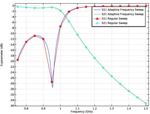
Analyze the same filter model with a much finer frequency resolution using Adaptive Frequency Sweep based on asymptotic waveform evaluation (AWE). When a device presents a slowly varying frequency response, the AWE method provides a faster solution time when running the simulation on many frequency points. The following example with the Adaptive Frequency Sweep can be computed about ten times faster than regular Frequency Domain sweeps with a same finer frequency resolution.
Electromagnetic Waves, Frequency Domain (emw)
Lumped Port 1
1
In the Model Builder window, under Component 1 (comp1) > Electromagnetic Waves, Frequency Domain (emw) click Lumped Port 1.
2
In the Settings window for Lumped Port, locate the Boundary Selection section.
3
Click  Create Selection.
4
In the Create Selection dialog, type Lumped port 1 in the Selection name text field.
5
Lumped Port 2
1
In the Model Builder window, click Lumped Port 2.
2
In the Settings window for Lumped Port, locate the Boundary Selection section.
3
Click  Create Selection.
4
In the Create Selection dialog, type Lumped port 2 in the Selection name text field.
5
Add Study
1
In the Home toolbar, click  Add Study to open the Add Study window.
2
Go to the Add Study window.
3
Find the Physics interfaces in study subsection. In the table, clear the Solve checkbox for Solid Mechanics (solid).
4
Find the Studies subsection. In the Select Study tree, select Preset Studies for Selected Physics Interfaces > Adaptive Frequency Sweep.
5
Click the Add Study button in the window toolbar.
6
In the Home toolbar, click  Add Study to close the Add Study window.
Study 3
Step 1: Adaptive Frequency Sweep
1
In the Settings window for Adaptive Frequency Sweep, locate the Study Settings section.
2
In the Frequencies text field, type range(fstart,fstep/20,fstop).
Use a 10 times finer frequency resolution.
A slowly varying scalar value curve works well for AWE expressions. When AWE expression type is set to Physics controlled in the Adaptive Frequency Sweep study settings, abs(comp1.emw.S21) is used automatically for two-port devices.
3
Locate the Physics and Variables Selection section. In the Solve for column of the table, under Component 1 (comp1), clear the checkboxes for Solid Mechanics (solid) and Moving Mesh.
Because such a fine frequency step generates a memory-intensive solution, the model file size will increase tremendously when it is saved. When only the frequency response of port related variables are of interest, it is not necessary to store all of the field solutions. By selecting the Store in Output checkbox in the Values of Dependent Variables section, we can control the part of the model on which the computed solution is saved. We only add the selection containing these boundaries where the port variables are calculated. The lumped port size is typically very small compared to the entire modeling domain, and the saved file size with the fine frequency step is more or less that of the regular discrete frequency sweep model when only the solutions on the port boundaries are stored.
4
Click to expand the Store in Output section. In the table, enter the following settings:
5
6
Under Selections, click  Add.
7
In the Add dialog, in the Selections list, choose Lumped port 1 and Lumped port 2.
8
It is necessary to include the lumped port boundaries to calculate S-parameters. By choosing only the lumped port boundaries for Store in Output settings, it is possible to reduce the size of a model file a lot.
9
In the Settings window for Adaptive Frequency Sweep, locate the Store in Output section.
10
11
12
Under Selections, click  Add.
13
In the Add dialog, in the Selections list, choose Lumped port 1 and Lumped port 2.
14
15
In the Settings window for Adaptive Frequency Sweep, locate the Store in Output section.
16
17
18
Under Selections, click  Add.
19
In the Add dialog, in the Selections list, choose Lumped port 1 and Lumped port 2.
20
21
In the Study toolbar, click  Compute.
Results
Multislice 1
1
In the Model Builder window, expand the Electric Field (emw) 2 node.
2
Right-click Multislice 1 and choose Delete.
Surface 1
Right-click Electric Field (emw) 2 and choose Surface.
Selection 1
1
In the Model Builder window, right-click Surface 1 and choose Selection.
2
3
In the Electric Field (emw) 2 toolbar, click  Plot.
Global 1
1
In the Model Builder window, expand the S-Parameter (emw) 2 node, then click Global 1.
2
In the Settings window for Global, locate the y-Axis Data section.
3
Global 2
1
Right-click Results > S-Parameter (emw) 2 > Global 1 and choose Duplicate.
2
In the Settings window for Global, locate the Data section.
3
From the Dataset list, choose Study 1/Solution 1 (sol1).
4
Locate the y-Axis Data section. In the table, enter the following settings:
5
Click to expand the Coloring and Style section. Find the Line style subsection. From the Line list, choose Cycle.
6
Find the Line markers subsection. From the Marker list, choose Cycle.
7
In the S-Parameter (emw) 2 toolbar, click  Plot.
Compare the results from Adaptive Frequency Sweep to those from the regular discrete sweep.