|
|
|

|
1
|
|
2
|
|
3
|
Click Add.
|
|
4
|
Click
|
|
1
|
|
2
|
Go to the Add Study window.
|
|
3
|
Find the Studies subsection. In the Select Study tree, select Preset Studies for Selected Physics Interfaces > Boundary Mode Analysis.
|
|
4
|
Right-click and choose Add Study.
|
|
5
|
|
1
|
|
2
|
|
3
|
|
1
|
|
2
|
|
3
|
|
4
|
|
1
|
|
2
|
|
3
|
|
1
|
|
2
|
|
3
|
|
1
|
|
2
|
|
3
|
|
4
|
|
5
|
|
6
|
|
1
|
|
2
|
|
3
|
|
4
|
|
5
|
|
6
|
Click
|
|
7
|
|
1
|
|
2
|
|
3
|
|
4
|
|
5
|
|
6
|
|
1
|
|
2
|
|
3
|
|
4
|
|
5
|
|
6
|
|
1
|
|
2
|
|
3
|
|
4
|
|
5
|
|
1
|
|
2
|
Select the object r3 only.
|
|
3
|
|
4
|
|
5
|
|
1
|
|
2
|
|
3
|
|
4
|
On the object dif1, select Points 1, 2, 11, and 12 only.
|

|
1
|
|
2
|
|
4
|
Click
|
|
5
|
|
1
|
|
2
|
|
3
|
|
4
|
|
5
|
|
6
|
|
7
|
|
1
|
|
2
|
|
3
|
|
4
|
|
5
|
Click
|
|
1
|
|
2
|
|
3
|
|
1
|
|
2
|
Select the object wp2 only.
|
|
3
|
|
4
|
Select the Keep input objects checkbox.
|
|
5
|
|
6
|
|
7
|
|
1
|
|
1
|
|
1
|
|
3
|
|
4
|
|
5
|
Select the Analyze as a TEM field checkbox.
|
|
1
|
|
2
|
|
3
|
Click
|
|
1
|
|
3
|
|
4
|
|
5
|
Select the Analyze as a TEM field checkbox.
|
|
1
|
|
2
|
|
3
|
Click
|
|
1
|
In the Model Builder window, under Component 1 (comp1) right-click Materials and choose Blank Material.
|
|
2
|
|
1
|
|
2
|
|
3
|
Click
|
|
4
|
|
5
|
Click OK.
|
|
6
|
|
1
|
In the Model Builder window, expand the Component 1 (comp1) > Definitions node, then click Component 1 (comp1) > Mesh 1.
|
|
2
|
|
3
|
|
4
|
Click
|
|
1
|
|
2
|
|
3
|
|
1
|
|
2
|
|
1
|
|
2
|
|
1
|
|
2
|
|
3
|
|
4
|
|
5
|
|
6
|
|
7
|
|
1
|
|
2
|
|
3
|
|
1
|
In the Model Builder window, under Component 1 (comp1) > Electromagnetic Waves, Frequency Domain (emw) click Port 1.
|
|
2
|
|
3
|
Click
|
|
4
|
|
5
|
Click OK.
|
|
1
|
|
2
|
|
3
|
Click
|
|
4
|
|
5
|
Click OK.
|
|
1
|
|
2
|
Go to the Add Study window.
|
|
3
|
|
4
|
Click the Add Study button in the window toolbar.
|
|
5
|
|
1
|
In the Study toolbar, click
|
|
2
|
|
3
|
|
4
|
|
6
|
Click to expand the Store in Output section. In the table, enter the following settings:
|
|
8
|
|
9
|
|
10
|
Click OK.
|
|
11
|
|
1
|
|
2
|
|
1
|
|
2
|
|
1
|
|
2
|
|
3
|
|
4
|
|
1
|
|
2
|
|
3
|
|
1
|
|
2
|
|
1
|
|
2
|
|
3
|
|
4
|
Locate the y-Axis Data section. In the table, enter the following settings:
|
|
5
|
Click to expand the Coloring and Style section. Find the Line markers subsection. From the Marker list, choose Cycle.
|
|
6
|
|
1
|
|
2
|
In the Settings window for 1D Plot Group, type S-parameter with Graph Markers in the Label text field.
|
|
3
|
|
1
|
|
2
|
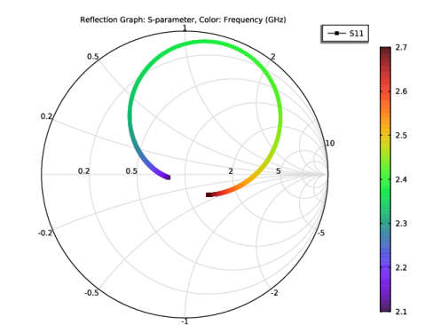
In the Settings window for Global, click Replace Expression in the upper-right corner of the y-Axis Data section. From the menu, choose Component 1 (comp1) > Electromagnetic Waves, Frequency Domain > Ports > S-parameter, dB - dB > emw.S11dB - S11.
|
|
1
|
|
2
|
|
3
|
|
4
|
|
5
|
Select the Show x-coordinate checkbox.
|
|
6
|
Select the Include unit checkbox.
|
|
7
|
|
1
|
|
2
|
In the Settings window for Global, click Replace Expression in the upper-right corner of the y-Axis Data section. From the menu, choose Component 1 (comp1) > Electromagnetic Waves, Frequency Domain > Ports > S-parameter, dB - dB > emw.S21dB - S21.
|
|
1
|
|
2
|
|
3
|
|
4
|
|
5
|
|
6
|
|
7
|
Select the Include unit checkbox.
|
|
8
|
|
9
|
Select the Show frame checkbox.
|
|
10
|