PDF

FEM–BEM Coupling of a Microstrip Patch Antenna
Introduction
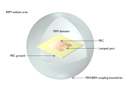
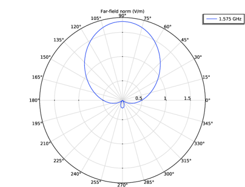
This example shows how to couple the finite element method (FEM), analyzing a microstrip patch antenna, to the boundary element method (BEM), for evaluating the field outside the FEM computational domain. The model computes the S-parameter, near-field distribution, and far-field radiation pattern through the FEM and the electric fields outside a given air domain sphere with the BEM.
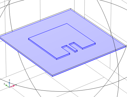
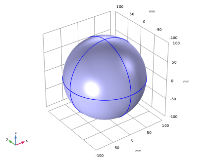
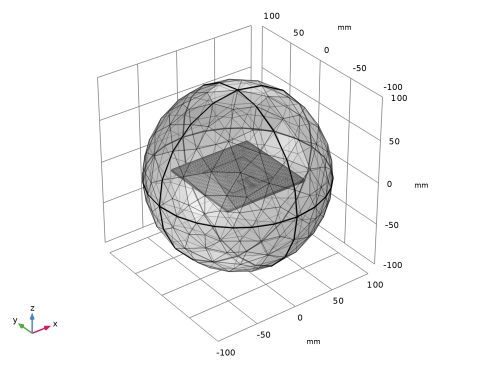
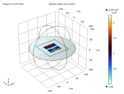
Figure 1: Model setup for the FEM–BEM coupling. One of the FEM–BEM coupling boundaries is removed from the view to show inside the FEM domains.
Model Definition
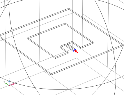
The FEM domains contain a microstrip patch antenna surrounded by an air domain. The antenna is excited by a uniform type lumped port that bridges the top feed line and bottom ground plane. A 60 mil substrate has a relative dielectric constant of 3.38. Additional details regarding the antenna design and impedance match are given in the Application Library example model Microstrip Patch Antenna. The outside of the FEM domains is set as infinite voids that are analyzed using the Electromagnetic Waves, Boundary Elements Interface. An Electric Field Coupling node under the Multiphysics branch addresses the coupling between FEM and BEM on the outermost boundaries of the FEM domains. For the conventional FEM-only analysis, an absorbing boundary condition such as a Scattering Boundary Condition is assigned on the outermost exterior boundaries to describe an open space for antenna analyses.
Results and Discussion
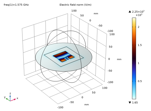
The computed S-parameter is below 20 dB indicating that the antenna input impedance is matched to the reference impedance of the lumped port (50 Ω). In Figure 2, strong electric fields are observed on the radiating edges.
Figure 2: The electric field norm is plotted on the xy-plane inside the FEM domains.
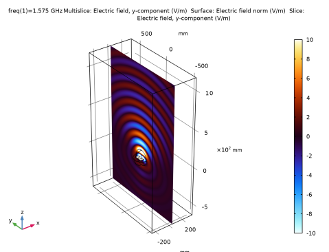
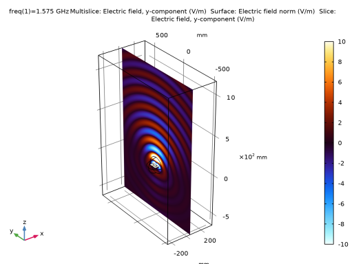
Figure 3: The y-component of the electric field outside the FEM domains are visualized using a Grid 3D dataset that can be configured to any size.
Figure 3 shows the smooth transition of the electric field from the FEM to the BEM surfaces visualizing the dominant polarization of the microstrip patch antenna.
Notes About the COMSOL Implementation
The model uses Only plot when requested functionality that is located at the Results node in the Model Builder. The visualization of BEM results often takes longer than the conventional FEM plots. This option may help saving time since it prevents any plot update until it is explicitly requested by clicking the Plot button.
Application Library path: RF_Module/Antennas/microstrip_patch_antenna_fem_bem
Modeling Instructions
From the File menu, choose New.
New
In the New window, click  Model Wizard.
Model Wizard
1
In the Model Wizard window, click  3D.
2
In the Select Physics tree, select Radio Frequency > Electromagnetic Waves, FEM-BEM.
3
Click Add.
4
Click  Study.
5
In the Select Study tree, select General Studies > Frequency Domain.
6
Geometry 1
1
In the Model Builder window, under Component 1 (comp1) click Geometry 1.
2
In the Settings window for Geometry, locate the Units section.
3
From the Length unit list, choose mm.
Study 1
Step 1: Frequency Domain
Define the study frequency ahead of performing any frequency-dependent operation such as building mesh. The physics-controlled mesh uses the specified frequency value.
1
In the Model Builder window, under Study 1 click Step 1: Frequency Domain.
2
In the Settings window for Frequency Domain, locate the Study Settings section.
3
In the Frequencies text field, type 1.575[GHz].
Global Definitions
Parameters 1
1
In the Model Builder window, under Global Definitions click Parameters 1.
2
In the Settings window for Parameters, locate the Parameters section.
3
Here mil refers to the unit milliinch, that is 1 mil = 0.0254 mm.
Geometry 1
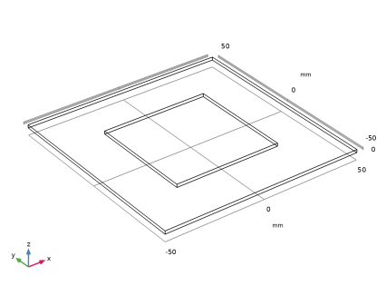
First, create the substrate block.
Substrate
1
In the Geometry toolbar, click  Block.
2
In the Settings window for Block, type Substrate in the Label text field.
3
Locate the Size and Shape section. In the Width text field, type w_sub.
4
In the Depth text field, type l_sub.
5
In the Height text field, type d.
6
Locate the Position section. From the Base list, choose Center.
7
Click  Build Selected.
Add the patch antenna.
Patch
1
In the Geometry toolbar, click  Block.
2
In the Settings window for Block, type Patch in the Label text field.
3
Locate the Size and Shape section. In the Width text field, type w_patch.
4
In the Depth text field, type l_patch.
5
In the Height text field, type d.
6
Locate the Position section. From the Base list, choose Center.
7
Click  Build Selected.
Choose wireframe rendering to get a better view of the interior parts.
8
Click the  Wireframe Rendering button in the Graphics toolbar.
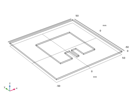
Create the impedance matching parts and a 50Ω feed line.
Stub
1
In the Geometry toolbar, click  Block.
2
In the Settings window for Block, type Stub in the Label text field.
3
Locate the Size and Shape section. In the Width text field, type w_stub.
4
In the Depth text field, type l_stub.
5
In the Height text field, type d.
6
Locate the Position section. From the Base list, choose Center.
7
In the x text field, type w_stub/2+w_line/2.
8
In the y text field, type l_stub/2-l_patch/2.
Copy 1 (copy1)
1
In the Geometry toolbar, click  Transforms and choose Copy.
2
3
In the Settings window for Copy, locate the Displacement section.
4
In the x text field, type -w_stub-w_line.
Difference 1 (dif1)
1
In the Geometry toolbar, click  Booleans and Partitions and choose Difference.
2
3
In the Settings window for Difference, locate the Difference section.
4
Click to select the  Activate Selection toggle button for Objects to subtract.
5
Select the objects blk3 and copy1 only.
6
Click  Build Selected.
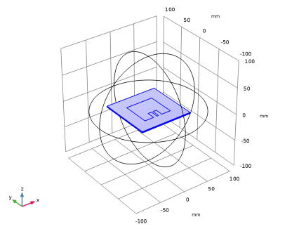
Add a sphere for the surrounding air.
Sphere 1 (sph1)
1
In the Geometry toolbar, click  Sphere.
2
In the Settings window for Sphere, locate the Size section.
3
In the Radius text field, type l_sub.
4
Click  Build All Objects.
5
Click the  Zoom Extents button in the Graphics toolbar.
Add Material
1
In the Home toolbar, click  Add Material to open the Add Material window.
2
Go to the Add Material window.
3
In the tree, select Built-in > Air.
4
Click the Add to Component button in the window toolbar.
5
In the Home toolbar, click  Add Material to close the Add Material window.
Materials
Air (mat1)
1
In the Settings window for Material, locate the Geometric Entity Selection section.
2
From the Selection list, choose All domains and voids.
Include voids for the BEM analysis.
Substrate
1
In the Model Builder window, right-click Materials and choose Blank Material.
2
In the Settings window for Material, type Substrate in the Label text field.
3
4
Locate the Material Contents section. In the table, enter the following settings:
Electromagnetic Waves, Frequency Domain (emw)
Perfect Electric Conductor 2
1
In the Physics toolbar, click  Boundaries and choose Perfect Electric Conductor.
2
Click the  Zoom In button in the Graphics toolbar, a couple of times to get a view of the antenna structure.
3
Lumped Port 1
1
In the Physics toolbar, click  Boundaries and choose Lumped Port.
2
Far-Field Domain 1
1
In the Physics toolbar, click  Domains and choose Far-Field Domain.
2
In the Settings window for Far-Field Domain, locate the Domain Selection section.
3
Click  Clear Selection.
4
5
Click the  Zoom Out button in the Graphics toolbar.
Far-Field Calculation 1
1
In the Model Builder window, expand the Far-Field Domain 1 node, then click Far-Field Calculation 1.
2
In the Settings window for Far-Field Calculation, locate the Boundary Selection section.
3
Click  Create Selection.
4
In the Create Selection dialog, type FEM-BEM coupling boundaries in the Selection name text field.
5
Electromagnetic Waves, Boundary Elements (embe)
1
In the Model Builder window, under Component 1 (comp1) click Electromagnetic Waves, Boundary Elements (embe).
2
In the Settings window for Electromagnetic Waves, Boundary Elements, locate the Domain Selection section.
3
From the Selection list, choose All voids.
Multiphysics
Electric Field Coupling 1 (elfc1)
1
In the Model Builder window, under Component 1 (comp1) > Multiphysics click Electric Field Coupling 1 (elfc1).
2
In the Settings window for Electric Field Coupling, locate the Boundary Selection section.
3
From the Selection list, choose FEM-BEM coupling boundaries.
Mesh 1
1
In the Model Builder window, under Component 1 (comp1) click Mesh 1.
2
In the Settings window for Mesh, locate the Sequence Type section.
3
From the list, choose Physics-controlled mesh.
4
Click  Build All.
Try to use transparency rendering.
5
Click the  Transparency button in the Graphics toolbar.
6
Click the  Transparency button in the Graphics toolbar.
Study 1
In the Study toolbar, click  Compute.
Results
Multislice 1
1
In the Model Builder window, expand the Results > Electric Field (emw) node, then click Multislice 1.
2
In the Settings window for Multislice, locate the Multiplane Data section.
3
Find the X-planes subsection. In the Planes text field, type 0.
4
Find the Y-planes subsection. In the Planes text field, type 0.
5
Locate the Coloring and Style section. From the Color table list, choose ThermalWaveDark.
Adjust the polar plot settings to generate the E-plane radiation pattern.
Radiation Pattern 1
1
In the Model Builder window, expand the Results > 2D Far Field (emw) node, then click Radiation Pattern 1.
2
In the Settings window for Radiation Pattern, locate the Evaluation section.
3
Find the Normal vector subsection. In the x text field, type 1.
4
In the z text field, type 0.
5
Find the Reference direction subsection. In the x text field, type 0.
6
In the y text field, type 1.
7
In the 2D Far Field (emw) toolbar, click  Plot.
Multislice 1
1
In the Model Builder window, expand the Electric Field, Domains (embe) node, then click Multislice 1.
2
In the Settings window for Multislice, locate the Expression section.
3
In the Expression text field, type embe.Ey.
4
Locate the Coloring and Style section. From the Color table list, choose ThermalWaveDark.
The BEM solution is visualized using the Grid 3D 1 dataset. Resize and enhance the resolution.
Grid 3D 1
1
In the Model Builder window, expand the Results > Datasets node, then click Grid 3D 1.
2
In the Settings window for Grid 3D, locate the Parameter Bounds section.
3
Find the Second parameter subsection. In the Minimum text field, type -600.
4
In the Maximum text field, type 600.
5
Find the Third parameter subsection. In the Minimum text field, type -600.
6
In the Maximum text field, type 1200.
7
Click to expand the Grid section. In the x resolution text field, type 2.
8
In the y resolution text field, type 600.
9
In the z resolution text field, type 1200.
The visualization of BEM results often takes longer than typical FEM cases. By checking Only plot when requested, the plot is not instantly updated when changing the settings. Finalize the plot settings first and then click the Plot button to see the results.
10
In the Model Builder window, click Results.
11
In the Settings window for Results, locate the Update of Results section.
12
Select the Only plot when requested checkbox.
Multislice 1
1
In the Model Builder window, under Results > Electric Field, Domains (embe) click Multislice 1.
2
In the Settings window for Multislice, locate the Multiplane Data section.
3
Find the y-planes subsection. In the Planes text field, type 0.
4
Find the z-planes subsection. In the Planes text field, type 0.
5
Click to expand the Range section. Select the Manual color range checkbox.
6
In the Minimum text field, type -10.
7
In the Maximum text field, type 10.
Surface 1
1
In the Model Builder window, click Surface 1.
2
In the Settings window for Surface, locate the Data section.
3
From the Dataset list, choose Study 1/Solution 1 (sol1).
4
Locate the Expression section. In the Expression text field, type emw.normE.
Selection 1
1
Right-click Surface 1 and choose Selection.
2
In the Settings window for Selection, locate the Selection section.
3
Click  Paste Selection.
4
In the Paste Selection dialog, type 5-9, 12, 13, 28 in the Selection text field.
5
Slice 1
1
In the Model Builder window, right-click Electric Field, Domains (embe) and choose Slice.
2
In the Settings window for Slice, locate the Data section.
3
From the Dataset list, choose Study 1/Solution 1 (sol1).
4
Locate the Expression section. In the Expression text field, type emw.Ey.
5
Locate the Plane Data section. In the Planes text field, type 1.
6
Click to expand the Inherit Style section. From the Plot list, choose Multislice 1.
7
In the Electric Field, Domains (embe) toolbar, click  Plot.
Note that the surface current plot in other plot groups can be physically meaningful when it is visualized on perfect electric conductor boundaries representing metallic surfaces outside the FEM domains.
Check the computed S-parameter value.