


PDF

Impedance Matching of a Lossy Ferrite 3-Port Circulator
Introduction
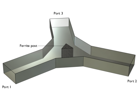
A microwave circulator is a nonreciprocal multiport device. It has the property that a wave incident on port 1 is routed into port 3 yet a wave incident on port 3 is not routed back into port 1 but is instead routed into port 2, and so on. This property of a circulator is used to isolate microwave components from each other, for example, when connecting a transmitter and a receiver to a common antenna. By connecting the transmitter, receiver, and antenna to different ports of a circulator, the transmitted power is routed to the antenna whereas any power received by the antenna goes into the receiver. Circulators typically rely on the use of ferrites, a special type of highly permeable and low-loss magnetic material that is anisotropic for a small RF signal when biased by a much larger static magnetic field. In the example, a three-port circulator is constructed from three rectangular waveguide sections joining at 120° and with a ferrite post inserted at the center of the joint.
Figure 1: The post is magnetized by a static H0 bias field along its axis. The bias field is supplied by external permanent magnets which are not explicitly modeled in this example.
Impedance Matching
An important step in the design of any microwave device is to match its input impedance for a given operating frequency. Impedance matching is equivalent to minimizing the reflections back to the inport. The parameters that need to be determined are the size of the ferrite post and the width of the wider waveguide section surrounding the ferrite. In this tutorial, these are varied in order to minimize the reflectance. The scattering parameters (S-parameters) used as measures of the reflectance and transmittance of the circulator are automatically computed.
The nominal frequency for the design of the device is chosen as 3 GHz. The circulator can be expected to perform reasonably well in a narrow frequency band around 3 GHz, and so a frequency range of 2.83.2 GHz is studied. It is desired that the device operates in single mode. Thus a rectangular waveguide cross section of 6.67 cm by 3.33 cm is selected to set the cutoff frequency for the fundamental TE10 mode to 2.25 GHz. The cutoff frequencies for the two nearest higher modes, the TE20 and TE01 modes, are both at 4.5 GHz, leaving a reasonable safety margin.
Model Definition
One of the rectangular ports is excited by the fundamental TE10 mode. At the ports, the boundaries are transparent to the TE10 mode. The following equation applies to the electric field vector E inside the circulator:
where μr denotes the relative permeability tensor, ω is the angular frequency, σ is the conductivity tensor, ε0 is the permittivity of vacuum, εr is the relative permittivity tensor, and k0 is the free space wave number. In this particular model, the conductivity is zero everywhere. Losses in the ferrite are defined using the loss tangent and the complex-valued permeability tensor. The magnetic permeability is of key importance as it is the anisotropy of this parameter that is responsible for the nonreciprocal behavior of the circulator. The material expressions are discussed in the next section for reference.
The Lossy Ferrite Material Model
Complete treatises on the theory of magnetic properties of ferrites can be found in Ref. 1 and Ref. 2. The model assumes that the static magnetic bias field, H0, is much stronger than the alternating magnetic field of the microwaves, so the quoted expressions are a linearization for a small-signal analysis around this operating point. Under these assumptions, and including losses, the anisotropic permeability of a ferrite magnetized in the positive z direction is given by
where
and the unique elements of the magnetic susceptibility tensor χ are given by
where
Here μ0 denotes the permeability of free space; ω is the angular frequency of the microwave field; ω0 is the precession resonance frequency (Larmor frequency) of a spinning electron in the applied magnetic bias field, H0; ωm is the electron Larmor frequency at the saturation magnetization of the ferrite, Ms; and γ is the gyromagnetic ratio of the electron. For a lossless ferrite (α = 0), the permeability becomes infinite at ω = ω0. In a lossy ferrite (α  0), this resonance becomes finite and is broadened. The damping factor, α, is related to the line width, ΔH, of the susceptibility curve near the resonance as given by the last expression above. The material data,
Ms = 5.41·104 A/m, εr = 14.5
with an effective loss tangent of 2·10-4 and ΔH = 3.18·103 A/m, are taken for aluminum garnet from Ref. 2. The applied bias field is set to H0 = 7.96·103 A/m. The electron gyromagnetic ratio taken from Ref. 2 is 1.759·1011 C/kg.
Results and Discussion
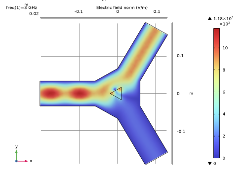
The default multislice plot shows the electric field norm. The electric field norm gives a good indication of where the main power is flowing and where there are standing waves due to reflections from the impedance mismatch at the center.
Figure 2: The default electric field norm plot shown on xy-plane.
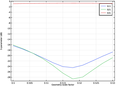
The plot of the S-parameter from the parametric sweep of sc_ferrite indicates a minimum for a scale factor of 0.518.
Figure 3: S-parameter as a function of sc_ferrite parameter.
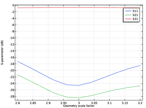
The plot of the S-parameter from the parametric sweep of sc_chamfer indicates a minimum for a scale factor of about 3.0.
Figure 4: S-parameter as a function of sc_chamfer parameter.
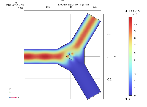
At the center frequency most of the standing waves are gone with the optimized values of sc_ferrite and sc_chamfer.
Figure 5: Electric field norm plot with the optimized sc_ferrite and sc_chamfer values.
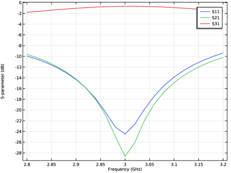
This is the frequency response of the final design.
Figure 6: S-parameter as a function of frequency with the optimized sc_ferrite and sc_chamfer values.
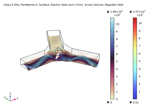
From the plot below, it should be possible to identify the model at first glance so it has to display the geometry and some characteristic simulation results.
Figure 7: 3D plot used for model thumbnail generation.
References
1. R.E. Collin, Foundations for Microwave Engineering, 2nd ed., IEEE Press/Wiley-Interscience, 2000.
2. D.M. Pozar, Microwave Engineering, 3rd ed., John Wiley & Sons Inc, 2004.
Application Library path: RF_Module/Ferrimagnetic_Devices/lossy_circulator_3d
Modeling Instructions
From the File menu, choose Open.
Browse to the model’s Application Libraries folder and double-click the file lossy_circulator_3d_geom.mph.
Definitions
Variables 1
1
In the Model Builder window, under Component 1 (comp1) right-click Definitions and choose Variables.
2
In the Settings window for Variables, locate the Variables section.
3
Geometry 1
Form Union (fin)
Next add material settings to the model. The lossy ferrite does not fit easily into the material settings so it will be taken care of later. Air is the only material to enter here.
Add Material
1
In the Materials toolbar, click  Add Material to open the Add Material window.
2
Go to the Add Material window.
3
In the tree, select Built-in > Air.
4
Click the Add to Component button in the window toolbar.
5
In the Materials toolbar, click  Add Material to close the Add Material window.
Materials
Air (mat1)
In the Electromagnetic Waves interface, the ferrite is entered as a separate, user-defined equation model referring to the global variables defined above.
Electromagnetic Waves, Frequency Domain (emw)
Wave Equation, Electric 2, Ferrite
1
In the Model Builder window, expand the Component 1 (comp1) > Electromagnetic Waves, Frequency Domain (emw) node.
2
Right-click Electromagnetic Waves, Frequency Domain (emw) and choose Wave Equation, Electric.
3
In the Settings window for Wave Equation, Electric, type Wave Equation, Electric 2, Ferrite in the Label text field.
4
5
Locate the Electric Displacement Field section. From the Electric displacement field model list, choose Loss tangent, dissipation factor.
6
From the ε′ list, choose User defined. In the associated text field, type 14.5.
7
From the tanδ list, choose User defined. In the associated text field, type 0.0002.
8
Locate the Magnetic Field section. From the μr list, choose User defined. From the list, choose Full.
9
Specify the μr matrix as
One inport for excitation and two outports need to be added next.
Port 1
1
In the Physics toolbar, click  Boundaries and choose Port.
2
3
In the Settings window for Port, locate the Port Properties section.
4
From the Type of port list, choose Rectangular.
For the first port, wave excitation is on by default.
Port 2
1
In the Physics toolbar, click  Boundaries and choose Port.
2
3
In the Settings window for Port, locate the Port Properties section.
4
From the Type of port list, choose Rectangular.
Port 3
1
In the Physics toolbar, click  Boundaries and choose Port.
2
3
In the Settings window for Port, locate the Port Properties section.
4
From the Type of port list, choose Rectangular.
The mesh needs to resolve the local wavelength and, for lossy domains, the skin depth. The skin depth in the ferrite is large so the main concern is to resolve the local wavelength. This is done by providing maximum mesh sizes per domain. The rule of thumb is to use a maximum element size that is one fifth of the local wavelength (at the maximum frequency) or smaller.
Mesh 1
Free Tetrahedral 1
In the Mesh toolbar, click  Free Tetrahedral.
Size 1
1
Right-click Free Tetrahedral 1 and choose Size.
2
In the Settings window for Size, locate the Geometric Entity Selection section.
3
From the Geometric entity level list, choose Domain.
4
5
Locate the Element Size section. Click the Custom button.
6
Locate the Element Size Parameters section.
7
Select the Maximum element size checkbox. In the associated text field, type 1.5e-2.
Size 2
1
In the Model Builder window, right-click Free Tetrahedral 1 and choose Size.
2
In the Settings window for Size, locate the Element Size section.
3
Click the Custom button.
4
Locate the Geometric Entity Selection section. From the Geometric entity level list, choose Domain.
5
6
Locate the Element Size Parameters section.
7
Select the Maximum element size checkbox. In the associated text field, type 4.5e-3.
8
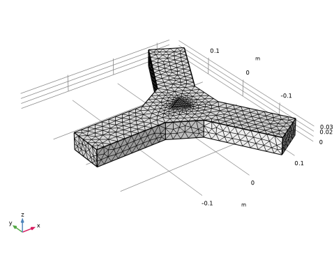
In the Model Builder window, right-click Mesh 1 and choose Build All.
The mesh should now look as in the above figure.
The final step in the model set up is to solve it for the nominal frequency and inspect the results for possible modeling errors.
Study 1
Step 1: Frequency Domain
1
In the Model Builder window, expand the Study 1 node, then click Step 1: Frequency Domain.
2
In the Settings window for Frequency Domain, locate the Study Settings section.
3
In the Frequencies text field, type 3[GHz].
4
In the Study toolbar, click  Compute.
Results
Electric Field (emw)
The default plot shows a slice plot of the electric field norm. It is best viewed from above.
1
Click the  Go to XY View button in the Graphics toolbar.
The electric field norm gives a good indication on where the main power is flowing and where there are standing waves due to reflections from the impedance mismatch at the center. See Figure 2.
The remaining work is to vary the two design parameters in order to minimize reflections at the nominal frequency. To do this, perform parametric sweeps over the design parameters (scale factors).
Study 1
Modify the study in order to vary the scale factor determining the size of the ferrite post. The study type is still Frequency Domain.
The parametric sweep over the scale factor is added as an extension to the frequency domain study.
Parametric Sweep
1
In the Study toolbar, click  Parametric Sweep.
2
In the Settings window for Parametric Sweep, locate the Study Settings section.
3
4
5
In the Study toolbar, click  Compute.
Results
Electric Field (emw) 1
Compare with the plot shown Figure 3. The plot of the S-parameter indicates a minimum for a scale factor of 0.518, so freeze the parameter at this value and add a new study for varying the next scale factor.
Global Definitions
Parameters 1
1
In the Model Builder window, under Global Definitions click Parameters 1.
2
In the Settings window for Parameters, locate the Parameters section.
3
Results
Global 1
1
In the Model Builder window, expand the Results > S-Parameter (emw) node, then click Global 1.
2
In the Settings window for Global, locate the x-Axis Data section.
3
In the Expression text field, type sc_chamfer.
Study 1
Parametric Sweep
1
In the Model Builder window, under Study 1 click Parametric Sweep.
2
In the Settings window for Parametric Sweep, locate the Study Settings section.
3
4
In the Study toolbar, click  Compute.
See Figure 4. The plot of the S-parameter indicates a minimum for a scale factor of about 3.0, so leave the parameter at this value and add a study for the frequency response.
Add Study
1
In the Study toolbar, click  Add Study to open the Add Study window.
2
Go to the Add Study window.
3
Find the Studies subsection. In the Select Study tree, select General Studies > Frequency Domain.
4
Click the Add Study button in the window toolbar.
5
In the Study toolbar, click  Add Study to close the Add Study window.
Study 2
Step 1: Frequency Domain
1
In the Settings window for Frequency Domain, locate the Study Settings section.
2
In the Frequencies text field, type range(2.8[GHz],20[MHz],3.2[GHz]).
3
In the Study toolbar, click  Compute.
Results
Electric Field (emw) 2
At the final frequency, there are pronounced standing waves. Change to the center frequency.
1
In the Settings window for 3D Plot Group, locate the Data section.
2
From the Parameter value (freq (GHz)) list, choose 3.
3
In the Electric Field (emw) 2 toolbar, click  Plot.
In the reproduced Figure 5 most of the standing waves are gone at the center frequency.
Finally plot all the S-parameters as a function of frequency.
Global 1
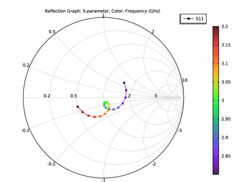
Reproduce Figure 6. This is the frequency response of the final design.
Now, let the solver excite one port at a time in order to get the full S-parameter matrix exported to a Touchstone file for potential use in a system simulation tool. The necessary steps are as follows:
Smith Plot (emw) 1
In the Model Builder window, expand the Results > S-Parameter (emw) 1 node, then click Results > Smith Plot (emw) 1.
Add Study
1
In the Home toolbar, click  Add Study to open the Add Study window.
2
Go to the Add Study window.
3
Find the Studies subsection. In the Select Study tree, select Preset Studies for Selected Physics Interfaces > Frequency Domain Source Sweep.
4
Click the Add Study button in the window toolbar.
5
In the Home toolbar, click  Add Study to close the Add Study window.
Study 3
Step 1: Frequency Domain Source Sweep
1
In the Settings window for Frequency Domain Source Sweep, locate the Study Settings section.
2
In the Frequencies text field, type 3[GHz].
3
In the Study toolbar, click  Compute.
Check the S-parameter matrix in a table.
Results
Electric Field, Logarithmic (emw) 2
As a final step, create a nice plot to use as a thumbnail. First change to the default 3D view and switch off grid.
1
Click the  Go to Default View button in the Graphics toolbar.
Definitions
View 5
1
In the Model Builder window, expand the Results > Derived Values node.
2
Right-click Component 1 (comp1) > Definitions and choose View.
3
In the Settings window for View, locate the View section.
4
Clear the Show grid checkbox.
Results
Electric Field (emw) 3
1
In the Model Builder window, under Results click Electric Field (emw) 3.
2
In the Settings window for 3D Plot Group, locate the Plot Settings section.
3
From the View list, choose View 5.
4
Click the  Go to Default View button in the Graphics toolbar.
5
In the Electric Field (emw) 3 toolbar, click  Plot.
Next, delete the Multislice plot and add a single slice.
Multislice 1
1
In the Model Builder window, expand the Electric Field (emw) 3 node.
2
Right-click Multislice 1 and choose Delete.
Surface 1
1
Right-click Electric Field (emw) 3 and choose Surface.
2
In the Settings window for Surface, locate the Expression section.
3
In the Expression text field, type emw.normE.
4
Locate the Coloring and Style section. From the Color table list, choose Avicularia.
Selection 1
1
Right-click Surface 1 and choose Selection.
2
Add deformation proportional to the electric field.
Deformation 1
1
In the Model Builder window, right-click Surface 1 and choose Deformation.
2
In the Settings window for Deformation, click Replace Expression in the upper-right corner of the Expression section. From the menu, choose Component 1 (comp1) > Electromagnetic Waves, Frequency Domain > Electric > emw.Ex,emw.Ey,emw.Ez - Electric field.
Electric Field (emw) 3
Display the magnetic field as arrows. Use logarithmic length scaling to make sure that the arrows are clearly visible everywhere. Place the arrows well above the slice.
Arrow Volume 1
1
In the Model Builder window, right-click Electric Field (emw) 3 and choose Arrow Volume.
2
In the Settings window for Arrow Volume, click Replace Expression in the upper-right corner of the Expression section. From the menu, choose Component 1 (comp1) > Electromagnetic Waves, Frequency Domain > Magnetic > emw.Hx,emw.Hy,emw.Hz - Magnetic field.
3
Locate the Expression section. Select the Description checkbox.
4
Locate the Arrow Positioning section. Find the X grid points subsection. In the Points text field, type 45.
5
Find the Y grid points subsection. In the Points text field, type 45.
6
Find the Z grid points subsection. From the Entry method list, choose Coordinates.
7
In the Coordinates text field, type 0.1/3.
8
Locate the Coloring and Style section. From the Arrow length list, choose Logarithmic.
Color Expression 1
1
Right-click Arrow Volume 1 and choose Color Expression.
2
In the Settings window for Color Expression, locate the Expression section.
3
In the Expression text field, type emw.normE.
4
In the Electric Field (emw) 3 toolbar, click  Plot.
While the arrow represents the direction of the magnetic field, the color indicates the strength of the electric field norm.
The port excitation can now be selected on the plot group. For the model thumbnail, select the second port.
Electric Field (emw) 3
1
In the Model Builder window, under Results click Electric Field (emw) 3.
2
In the Settings window for 3D Plot Group, locate the Data section.
3
From the Parameter value (PortName) list, choose 2.
4
In the Electric Field (emw) 3 toolbar, click  Plot.
By plotting Figure 7, conclude this modeling session.