|
|
|

|
1
|
|
2
|
|
3
|
Click Add.
|
|
4
|
Click
|
|
5
|
|
6
|
Click
|
|
1
|
|
2
|
|
3
|
Click
|
|
4
|
Browse to the model’s Application Libraries folder and double-click the file high_speed_interconnect_tdr_parameters.txt.
|
|
1
|
|
2
|
|
3
|
|
1
|
|
2
|
|
3
|
|
4
|
|
5
|
|
6
|
|
7
|
|
8
|
Click
|
|
9
|
|
1
|
|
2
|
|
3
|
|
4
|
|
5
|
|
6
|
|
1
|
|
2
|
Select the object r1 only.
|
|
3
|
|
4
|
|
5
|
Click
|
|
1
|
|
2
|
|
3
|
|
4
|
|
5
|
|
6
|
|
7
|
|
1
|
|
2
|
Click in the Graphics window and then press Ctrl+A to select both objects.
|
|
3
|
|
4
|
Clear the Keep interior boundaries checkbox.
|
|
5
|
|
1
|
|
2
|
|
1
|
|
2
|
Click in the Graphics window and then press Ctrl+A to select both objects.
|
|
3
|
|
4
|
Select the Keep input objects checkbox.
|
|
5
|
|
1
|
|
2
|
|
3
|
|
4
|
|
5
|
|
6
|
|
1
|
|
2
|
|
3
|
|
4
|
|
1
|
|
2
|
|
3
|
|
1
|
|
2
|
|
3
|
|
1
|
|
2
|
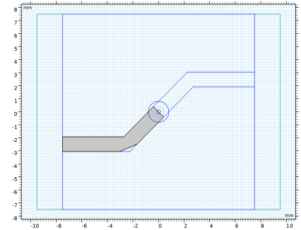
Select the object wp2 only.
|
|
3
|
|
4
|
|
5
|
Click
|
|
1
|
|
2
|
|
3
|
|
4
|
|
1
|
|
2
|
|
3
|
|
4
|
|
5
|
|
6
|
|
7
|
Click to expand the Layers section. In the table, enter the following settings:
|
|
8
|
|
9
|
Select the Right checkbox.
|
|
10
|
Clear the Bottom checkbox.
|
|
11
|
|
12
|
|
13
|
|
1
|
|
2
|
|
3
|
|
1
|
|
2
|
|
3
|
|
4
|
Locate the Units section. In the table, enter the following settings:
|
|
5
|
|
1
|
In the Model Builder window, under Component 1 (comp1) right-click Materials and choose Blank Material.
|
|
2
|
|
1
|
|
2
|
|
3
|
Click
|
|
4
|
|
5
|
|
6
|
|
1
|
|
2
|
|
3
|
Click
|
|
4
|
In the Paste Selection dialog, type 14, 21-22, 25, 34-35, 38, 41-44, 46-47, 51, 54, 58-59, 61 in the Selection text field.
|
|
5
|
|
1
|
|
2
|
|
3
|
Click
|
|
4
|
In the Paste Selection dialog, type 1-5, 7-8, 10, 13, 16, 18, 26-29, 67-68, 72, 75-76 in the Selection text field.
|
|
5
|
|
1
|
|
3
|
|
4
|
Click
|
|
5
|
|
6
|
|
7
|
|
1
|
|
1
|
|
2
|
|
3
|
|
4
|
|
5
|
Locate the Physics-Controlled Mesh section. In the table, clear the Use checkbox for Geometric Analysis, Detail Size.
|
|
6
|
|
1
|
|
2
|
|
3
|
Click the Custom button.
|
|
4
|
|
5
|
|
6
|
|
1
|
|
2
|
|
3
|
Click
|
|
4
|
Click
|
|
5
|
|
6
|
|
7
|
|
8
|
|
9
|
|
1
|
|
2
|
|
3
|
|
4
|
Click
|
|
5
|
|
6
|
|
7
|
|
8
|
Click the Custom button.
|
|
9
|
Locate the Element Size Parameters section.
|
|
10
|
|
11
|
|
12
|
|
1
|
|
1
|
|
2
|
|
1
|
|
2
|
|
3
|
|
4
|
Click to expand the Store in Output section. In the table, enter the following settings:
|
|
6
|
|
7
|
|
8
|
Click OK.
|
|
9
|
|
10
|
|
11
|
Clear the Generate default plots checkbox.
|
|
1
|
|
2
|
|
3
|
|
4
|
|
5
|
|
6
|
|
1
|
|
2
|
|
3
|
|
4
|
|
5
|
|
1
|
|
2
|
|
4
|
Click to expand the Coloring and Style section. Find the Line markers subsection. From the Marker list, choose Cycle.
|
|
5
|
|
1
|
|
2
|
In the Settings window for Global, click Add Expression in the upper-right corner of the y-Axis Data section. From the menu, choose Component 1 (comp1) > Electromagnetic Waves, Transient > Ports > Voltage > temw.Vport_1 - Lumped port 1 voltage - V.
|
|
3
|
|
1
|
|
2
|
|
3
|
|
4
|
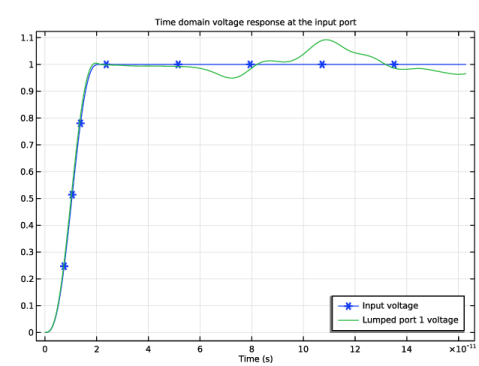
In the Times (s) list, choose 4.1667E-13, 8.3333E-13, 1.25E-12, 1.6667E-12, 2.0833E-12, 2.5E-12, 2.9167E-12, 3.3333E-12, 3.75E-12, 4.1667E-12, 4.5833E-12, 5E-12, 5.4167E-12, 5.8333E-12, 6.25E-12, 6.6667E-12, 7.0833E-12, 7.5E-12, 7.9167E-12, 8.3333E-12, 8.75E-12, 9.1667E-12, 9.5833E-12, 1E-11, 1.0417E-11, 1.0833E-11, 1.125E-11, 1.1667E-11, 1.2083E-11, 1.25E-11, 1.2917E-11, 1.3333E-11, 1.375E-11, 1.4167E-11, 1.4583E-11, 1.5E-11, 1.5417E-11, 1.5833E-11, 1.625E-11, 1.6667E-11, 1.7083E-11, 1.75E-11, 1.7917E-11, 1.8333E-11, 1.875E-11, 1.9167E-11, 1.9583E-11, 2E-11, 2.0417E-11, 2.0833E-11, 2.125E-11, 2.1667E-11, 2.2083E-11, 2.25E-11, 2.2917E-11, 2.3333E-11, 2.375E-11, 2.4167E-11, 2.4583E-11, 2.5E-11, 2.5417E-11, 2.5833E-11, 2.625E-11, 2.6667E-11, 2.7083E-11, 2.75E-11, 2.7917E-11, 2.8333E-11, 2.875E-11, 2.9167E-11, 2.9583E-11, 3E-11, 3.0417E-11, 3.0833E-11, 3.125E-11, 3.1667E-11, 3.2083E-11, 3.25E-11, 3.2917E-11, 3.3333E-11, 3.375E-11, 3.4167E-11, 3.4583E-11, 3.5E-11, 3.5417E-11, 3.5833E-11, 3.625E-11, 3.6667E-11, 3.7083E-11, 3.75E-11, 3.7917E-11, 3.8333E-11, 3.875E-11, 3.9167E-11, 3.9583E-11, 4E-11, 4.0417E-11, 4.0833E-11, 4.125E-11, 4.1667E-11, 4.2083E-11, 4.25E-11, 4.2917E-11, 4.3333E-11, 4.375E-11, 4.4167E-11, 4.4583E-11, 4.5E-11, 4.5417E-11, 4.5833E-11, 4.625E-11, 4.6667E-11, 4.7083E-11, 4.75E-11, 4.7917E-11, 4.8333E-11, 4.875E-11, 4.9167E-11, 4.9583E-11, 5E-11, 5.0417E-11, 5.0833E-11, 5.125E-11, 5.1667E-11, 5.2083E-11, 5.25E-11, 5.2917E-11, 5.3333E-11, 5.375E-11, 5.4167E-11, 5.4583E-11, 5.5E-11, 5.5417E-11, 5.5833E-11, 5.625E-11, 5.6667E-11, 5.7083E-11, 5.75E-11, 5.7917E-11, 5.8333E-11, 5.875E-11, 5.9167E-11, 5.9583E-11, 6E-11, 6.0417E-11, 6.0833E-11, 6.125E-11, 6.1667E-11, 6.2083E-11, 6.25E-11, 6.2917E-11, 6.3333E-11, 6.375E-11, 6.4167E-11, 6.4583E-11, 6.5E-11, 6.5417E-11, 6.5833E-11, 6.625E-11, 6.6667E-11, 6.7083E-11, 6.75E-11, 6.7917E-11, 6.8333E-11, 6.875E-11, 6.9167E-11, 6.9583E-11, 7E-11, 7.0417E-11, 7.0833E-11, 7.125E-11, 7.1667E-11, 7.2083E-11, 7.25E-11, 7.2917E-11, 7.3333E-11, 7.375E-11, 7.4167E-11, 7.4583E-11, 7.5E-11, 7.5417E-11, 7.5833E-11, 7.625E-11, 7.6667E-11, 7.7083E-11, 7.75E-11, 7.7917E-11, 7.8333E-11, 7.875E-11, 7.9167E-11, 7.9583E-11, 8E-11, 8.0417E-11, 8.0833E-11, 8.125E-11, 8.1667E-11, 8.2083E-11, 8.25E-11, 8.2917E-11, 8.3333E-11, 8.375E-11, 8.4167E-11, 8.4583E-11, 8.5E-11, 8.5417E-11, 8.5833E-11, 8.625E-11, 8.6667E-11, 8.7083E-11, 8.75E-11, 8.7917E-11, 8.8333E-11, 8.875E-11, 8.9167E-11, 8.9583E-11, 9E-11, 9.0417E-11, 9.0833E-11, 9.125E-11, 9.1667E-11, 9.2083E-11, 9.25E-11, 9.2917E-11, 9.3333E-11, 9.375E-11, 9.4167E-11, 9.4583E-11, 9.5E-11, 9.5417E-11, 9.5833E-11, 9.625E-11, 9.6667E-11, 9.7083E-11, 9.75E-11, 9.7917E-11, 9.8333E-11, 9.875E-11, 9.9167E-11, 9.9583E-11, 1E-10, 1.0042E-10, 1.0083E-10, 1.0125E-10, 1.0167E-10, 1.0208E-10, 1.025E-10, 1.0292E-10, 1.0333E-10, 1.0375E-10, 1.0417E-10, 1.0458E-10, 1.05E-10, 1.0542E-10, 1.0583E-10, 1.0625E-10, 1.0667E-10, 1.0708E-10, 1.075E-10, 1.0792E-10, 1.0833E-10, 1.0875E-10, 1.0917E-10, 1.0958E-10, 1.1E-10, 1.1042E-10, 1.1083E-10, 1.1125E-10, 1.1167E-10, 1.1208E-10, 1.125E-10, 1.1292E-10, 1.1333E-10, 1.1375E-10, 1.1417E-10, 1.1458E-10, 1.15E-10, 1.1542E-10, 1.1583E-10, 1.1625E-10, 1.1667E-10, 1.1708E-10, 1.175E-10, 1.1792E-10, 1.1833E-10, 1.1875E-10, 1.1917E-10, 1.1958E-10, 1.2E-10, 1.2042E-10, 1.2083E-10, 1.2125E-10, 1.2167E-10, 1.2208E-10, 1.225E-10, 1.2292E-10, 1.2333E-10, 1.2375E-10, 1.2417E-10, 1.2458E-10, 1.25E-10, 1.2542E-10, 1.2583E-10, 1.2625E-10, 1.2667E-10, 1.2708E-10, 1.275E-10, 1.2792E-10, 1.2833E-10, 1.2875E-10, 1.2917E-10, 1.2958E-10, 1.3E-10, 1.3042E-10, 1.3083E-10, 1.3125E-10, 1.3167E-10, 1.3208E-10, 1.325E-10, 1.3292E-10, 1.3333E-10, 1.3375E-10, 1.3417E-10, 1.3458E-10, 1.35E-10, 1.3542E-10, 1.3583E-10, 1.3625E-10, 1.3667E-10, 1.3708E-10, 1.375E-10, 1.3792E-10, 1.3833E-10, 1.3875E-10, 1.3917E-10, 1.3958E-10, 1.4E-10, 1.4042E-10, 1.4083E-10, 1.4125E-10, 1.4167E-10, 1.4208E-10, 1.425E-10, 1.4292E-10, 1.4333E-10, 1.4375E-10, 1.4417E-10, 1.4458E-10, 1.45E-10, 1.4542E-10, 1.4583E-10, 1.4625E-10, 1.4667E-10, 1.4708E-10, 1.475E-10, 1.4792E-10, 1.4833E-10, 1.4875E-10, 1.4917E-10, 1.4958E-10, 1.5E-10, 1.5042E-10, 1.5083E-10, 1.5125E-10, 1.5167E-10, 1.5208E-10, 1.525E-10, 1.5292E-10, 1.5333E-10, 1.5375E-10, 1.5417E-10, 1.5458E-10, 1.55E-10, 1.5542E-10, 1.5583E-10, 1.5625E-10, 1.5667E-10, 1.5708E-10, 1.575E-10, 1.5792E-10, 1.5833E-10, 1.5875E-10, 1.5917E-10, 1.5958E-10, 1.6E-10, 1.6042E-10, 1.6083E-10, 1.6125E-10, 1.6167E-10, 1.6208E-10, 1.625E-10, and 1.6292E-10.
|
|
5
|
|
6
|
|
7
|
|
1
|
|
2
|
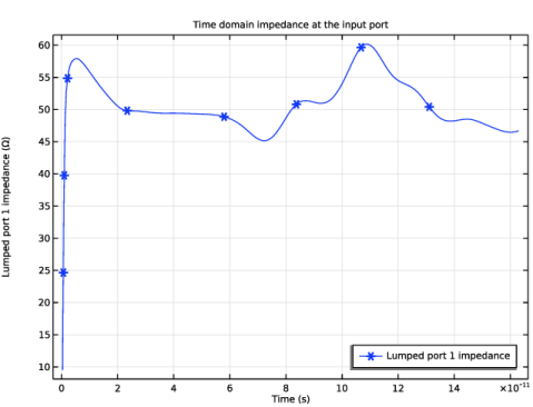
In the Settings window for Global, click Add Expression in the upper-right corner of the y-Axis Data section. From the menu, choose Component 1 (comp1) > Electromagnetic Waves, Transient > Ports > Impedance > temw.Zport_1 - Lumped port 1 impedance - Ω.
|
|
3
|
Locate the Coloring and Style section. Find the Line markers subsection. From the Marker list, choose Cycle.
|
|
4
|
|
5
|
|
1
|
|
2
|
On the object uni1, select Point 4 only.
|
|
3
|
|
4
|
|
5
|
|
1
|
|
2
|
|
3
|
|
4
|
|
1
|
In the Model Builder window, under Study 1 > Solver Configurations right-click Solution 1 (sol1) and choose Solution > Copy.
|
|
2
|
|
1
|
|
2
|
|
3
|
|
4
|
Click Add Expression in the upper-right corner of the y-Axis Data section. From the menu, choose Component 1 (comp1) > Electromagnetic Waves, Transient > Ports > Voltage > temw.Vport_1 - Lumped port 1 voltage - V.
|
|
5
|
Locate the y-Axis Data section. In the table, enter the following settings:
|
|
6
|
|
1
|
In the Model Builder window, under Results > 1D Plot Group 2 right-click Global 1 and choose Duplicate.
|
|
2
|
|
3
|
|
4
|
|
5
|
Locate the y-Axis Data section. In the table, enter the following settings:
|
|
6
|
|
1
|
|
2
|
|
3
|
Clear the Plot dataset edges checkbox.
|
|
4
|
|
1
|
|
2
|
|
3
|
|
1
|
|
2
|
Click
|
|
1
|
|
2
|
|
3
|
Click
|
|
4
|
In the Paste Selection dialog, type 14, 21, 22, 25, 35, 36, 39, 42-45, 47, 48, 52, 55, 59, 60, 62 in the Selection text field.
|
|
5
|
Click OK.
|
|
1
|
|
2
|
|
3
|
|
4
|
|
5
|
|
1
|
|
2
|
|
3
|
|
1
|
|
1
|
|
2
|
|
3
|
|
4
|