PDF

Frequency Selective Surface, Periodic Complementary Split Ring Resonator
Introduction
Frequency selective surfaces (FSSs) are periodic structures with a bandpass or a bandstop frequency response. This example shows that only signals around the center frequency can pass through the periodic complementary split ring resonator layer.
Figure 1: One unit cell of the complementary split ring resonator is modeled with periodic boundary conditions to simulate an infinite 2D array.
Model Definition
A split ring slot is patterned on a geometrically thin metal layer that sits on a 2 mm PTFE substrate (Figure 1). The metal layer is assumed to be much thicker than the skin depth in the simulated frequency range, so it is modeled as a perfect electric conductor (PEC). The rest of the simulation domain is filled with air.
Floquet-periodic boundary conditions are used on four sides of the unit cell to simulate the infinite 2D array.
The port boundary condition for excitation (source) is placed on the top of the simulation domain, while the observation (listener) port is on the bottom. The Port boundary conditions automatically determine the reflection and transmission characteristics in terms of S-parameters.
To make it simpler to handle the boundary conditions, a Periodic Structure node is used. It automatically adds and configures ports and periodic conditions as subnodes.
The periodic boundary condition requires identical surface meshes on paired boundaries. This is accomplished by using the Identical Face operation for the mesh on the paired boundaries. This mesh configuration is automatically set when using the physics-controlled mesh as shown in the step-by-step instructions. If you are interested in seeing more details about the mesh, build the physics-controlled mesh once and then change the mesh sequence type to the user-controlled mesh in the mesh settings. Then you can inspect the generated mesh sequence.
Results and Discussion
The modified multislice default plot (Figure 2) shows the electric field norm on the complementary split ring resonator. Strong fields are observed inside the slot. The S-parameter plot in Figure 3 shows that this periodic structure functions as a bandpass filter near 4.6 GHz. In Figure 4, the S-parameters appear as a function of incident angle and show that the periodic structure is penetrable at 4.6 GHz over the simulated range, except for grazing angles.
The resonance frequency of this periodic structure can be quickly evaluated as 4.59 GHz using an Eigenfrequency study, which is not included in this example.
Figure 2: The fields are confined in the split ring slot.
Figure 3: The S-parameter plot shows a bandpass resonance near 4.6 GHz.
Figure 4: The S-parameter plot is shown as a function of incident angle.
Application Library path: RF_Module/EMI_EMC_Applications/frequency_selective_surface_csrr
Modeling Instructions
From the File menu, choose New.
New
In the New window, click  Model Wizard.
Model Wizard
1
In the Model Wizard window, click  3D.
2
In the Select Physics tree, select Radio Frequency > Electromagnetic Waves, Frequency Domain (emw).
3
Click Add.
4
Click  Study.
5
In the Select Study tree, select General Studies > Frequency Domain.
6
Study 1
Step 1: Frequency Domain
1
In the Model Builder window, under Study 1 click Step 1: Frequency Domain.
2
In the Settings window for Frequency Domain, locate the Study Settings section.
3
In the Frequencies text field, type range(3.8[GHz],0.1[GHz],5.4[GHz]).
Global Definitions
Parameters 1
1
In the Model Builder window, under Global Definitions click Parameters 1.
2
In the Settings window for Parameters, locate the Parameters section.
3
Geometry 1
1
In the Model Builder window, under Component 1 (comp1) click Geometry 1.
2
In the Settings window for Geometry, locate the Units section.
3
From the Length unit list, choose mm.
Block 1 (blk1)
1
In the Geometry toolbar, click  Block.
2
In the Settings window for Block, locate the Size and Shape section.
3
In the Width text field, type 15.
4
In the Depth text field, type 15.
5
In the Height text field, type 45.
6
Locate the Position section. From the Base list, choose Center.
7
Click  Build Selected.
8
Click the  Wireframe Rendering button in the Graphics toolbar.
Work Plane 1 (wp1)
In the Geometry toolbar, click  Work Plane.
Work Plane 1 (wp1) > Plane Geometry
In the Model Builder window, click Plane Geometry.
Work Plane 1 (wp1) > Circle 1 (c1)
1
In the Work Plane toolbar, click  Circle.
2
In the Settings window for Circle, locate the Size and Shape section.
3
In the Radius text field, type 5.
4
Click  Build Selected.
5
Click the  Zoom Extents button in the Graphics toolbar.
Work Plane 1 (wp1) > Circle 2 (c2)
1
In the Work Plane toolbar, click  Circle.
2
In the Settings window for Circle, locate the Size and Shape section.
3
In the Radius text field, type 3.5.
Work Plane 1 (wp1) > Rectangle 1 (r1)
1
In the Work Plane toolbar, click  Rectangle.
2
In the Settings window for Rectangle, locate the Size and Shape section.
3
In the Width text field, type 4.
4
Locate the Position section. From the Base list, choose Center.
5
In the xw text field, type 4.
Work Plane 1 (wp1) > Difference 1 (dif1)
1
In the Work Plane toolbar, click  Booleans and Partitions and choose Difference.
2
3
In the Settings window for Difference, locate the Difference section.
4
Click to select the  Activate Selection toggle button for Objects to subtract.
5
Select the objects c2 and r1 only.
6
Click  Build Selected.
Block 2 (blk2)
1
In the Model Builder window, right-click Geometry 1 and choose Block.
2
In the Settings window for Block, locate the Size and Shape section.
3
In the Width text field, type 15.
4
In the Depth text field, type 15.
5
In the Height text field, type 2.
6
Locate the Position section. From the Base list, choose Center.
7
In the z text field, type -1.
8
Click  Build All Objects.
Electromagnetic Waves, Frequency Domain (emw)
Periodic Structure 1
1
In the Physics toolbar, click  Domains and choose Periodic Structure.
The Periodic Structure node automatically adds subnodes for the excitation port and the passive port on the transmission side. Furthermore, periodic boundary conditions of Floquet type are added.
2
In the Settings window for Periodic Structure, locate the Port Mode Settings section.
3
In the α1 text field, type theta.
4
From the list, choose Transverse magnetic (TM).
These settings allow for a sweep of the angle of incidence in the x z plane (the plane of incidence), with a polarization in the same plane of incidence.
Perfect Electric Conductor 2
1
In the Physics toolbar, click  Boundaries and choose Perfect Electric Conductor.
2
In the Settings window for Perfect Electric Conductor, locate the Boundary Selection section.
3
Click  Clear Selection.
4
Add Material
1
In the Materials toolbar, click  Add Material to open the Add Material window.
2
Go to the Add Material window.
3
In the tree, select Built-in > Air.
4
Click the Add to Component button in the window toolbar.
5
In the Materials toolbar, click  Add Material to close the Add Material window.
Materials
Dielectric
1
In the Model Builder window, under Component 1 (comp1) right-click Materials and choose Blank Material.
2
In the Settings window for Material, type Dielectric in the Label text field.
3
4
Locate the Material Contents section. In the table, enter the following settings:
Mesh 1
1
In the Model Builder window, under Component 1 (comp1) right-click Mesh 1 and choose Build All.
2
Click the  Zoom Extents button in the Graphics toolbar.
3
In the Settings window for Mesh, locate the Physics-Controlled Mesh section.
4
From the Element size list, choose Extremely fine.
5
Click  Build All.
Definitions
Hide for Physics 1
1
In the Model Builder window, expand the Component 1 (comp1) > Definitions node.
2
Right-click View 1 and choose Hide for Physics.
3
In the Settings window for Hide for Physics, locate the Geometric Entity Selection section.
4
From the Geometric entity level list, choose Boundary.
5
Mesh 1
In the Model Builder window, click Mesh 1.
1
In the Model Builder window, under Component 1 (comp1) click Mesh 1.
Study 1
In the Study toolbar, click  Compute.
Results
Electric Field (emw)
1
In the Settings window for 3D Plot Group, locate the Data section.
2
From the Parameter value (freq (GHz)) list, choose 4.6.
Multislice 1
1
In the Model Builder window, expand the Electric Field (emw) node, then click Multislice 1.
2
In the Settings window for Multislice, locate the Multiplane Data section.
3
Find the X-planes subsection. In the Planes text field, type 0.
4
Find the Y-planes subsection. In the Planes text field, type 0.
5
Find the Z-planes subsection. From the Entry method list, choose Coordinates.
6
In the Coordinates text field, type -1.
7
In the Electric Field (emw) toolbar, click  Plot.
8
Click the  Zoom In button in the Graphics toolbar twice.
This reproduces Figure 2.
S-Parameter (emw)
1
In the Model Builder window, under Results click S-Parameter (emw).
Identify the resonant frequency of the periodic structure from the S-parameter plot Figure 3.
Smith Plot (emw)
In the Model Builder window, click Smith Plot (emw).
Electric Field, Logarithmic (emw)
In the Model Builder window, click Electric Field, Logarithmic (emw).
Next, evaluate the reflectivity and transmittivity performance of the model with different incident angles.
Add Study
1
In the Home toolbar, click  Add Study to open the Add Study window.
2
Go to the Add Study window.
Study 1
Solver Configurations
1
Find the Studies subsection. In the Select Study tree, select General Studies > Frequency Domain.
2
Click the Add Study button in the window toolbar.
If you want to clear the Add Study window after adding, click Add Study again in the Home toolbar.
3
In the Home toolbar, click  Add Study to close the Add Study window.
Study 2
Parametric Sweep
1
In the Study toolbar, click  Parametric Sweep.
2
In the Settings window for Parametric Sweep, locate the Study Settings section.
3
4
Step 1: Frequency Domain
1
In the Model Builder window, click Step 1: Frequency Domain.
2
In the Settings window for Frequency Domain, locate the Study Settings section.
3
In the Frequencies text field, type 4.6[GHz].
4
In the Study toolbar, click  Compute.
Results
Multislice 1
1
In the Model Builder window, expand the Electric Field (emw) 1 node, then click Multislice 1.
2
In the Settings window for Multislice, locate the Multiplane Data section.
3
Find the X-planes subsection. In the Planes text field, type 0.
4
Find the Y-planes subsection. In the Planes text field, type 0.
5
Find the Z-planes subsection. From the Entry method list, choose Coordinates.
6
In the Coordinates text field, type -1.
7
In the Electric Field (emw) 1 toolbar, click  Plot.
Global 1
1
In the Model Builder window, expand the Results > S-Parameter (emw) 1 node, then click Global 1.
2
In the Settings window for Global, locate the x-Axis Data section.
3
From the Unit list, choose °.
4
In the S-Parameter (emw) 1 toolbar, click  Plot.
This is the S-parameter plot as a function of incident angle shown in Figure 4.
Smith Plot (emw) 1
In the Model Builder window, expand the Smith Plot (emw) 1 node.
Color Expression 1
1
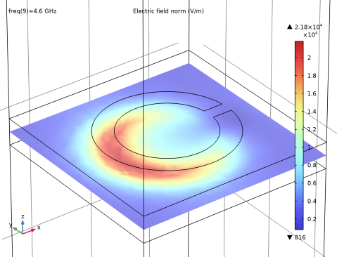
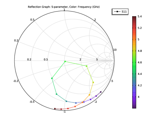
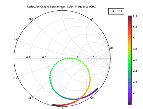
In the Model Builder window, expand the Results > Smith Plot (emw) 1 > Reflection Graph 1 node, then click Color Expression 1.
2
In the Settings window for Color Expression, locate the Expression section.
3
In the Expression text field, type theta.
4
From the Unit list, choose °.
Reflection Graph 1
1
In the Model Builder window, click Reflection Graph 1.
2
In the Settings window for Reflection Graph, click to expand the Title section.
3
In the Title text area, type Reflection Graph: S-parameter, Color: Elevation angle (degrees).
Analyze the same model with a much finer frequency resolution using Adaptive Frequency Sweep based on asymptotic waveform evaluation (AWE). When a device presents a slowly varying frequency response, the AWE provides a faster solution time when running the simulation on many frequency points. The following example with the AWE can be computed 50 times faster than regular Frequency Domain sweeps with a same finer frequency resolution.
Electromagnetic Waves, Frequency Domain (emw)
Periodic Port 1
1
In the Model Builder window, under Component 1 (comp1) > Electromagnetic Waves, Frequency Domain (emw) > Periodic Structure 1 click Periodic Port 1.
2
In the Settings window for Periodic Port, locate the Boundary Selection section.
3
Click  Create Selection.
4
In the Create Selection dialog, type Port 1 in the Selection name text field.
5
Periodic Port 2
1
In the Model Builder window, click Periodic Port 2.
2
In the Settings window for Periodic Port, locate the Boundary Selection section.
3
Click  Create Selection.
4
In the Create Selection dialog, type Port 2 in the Selection name text field.
5
Add Study
1
In the Home toolbar, click  Add Study to open the Add Study window.
2
Go to the Add Study window.
3
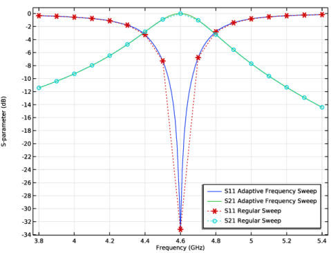
Find the Studies subsection. In the Select Study tree, select Preset Studies for Selected Physics Interfaces > Adaptive Frequency Sweep.
4
Click the Add Study button in the window toolbar.
5
In the Home toolbar, click  Add Study to close the Add Study window.
Study 3
Step 1: Adaptive Frequency Sweep
1
In the Settings window for Adaptive Frequency Sweep, locate the Study Settings section.
2
In the Frequencies text field, type range(3.8[GHz],0.01[GHz],5.4[GHz]).
Use a ten times finer frequency resolution.
A slowly varying scalar value curve works well for AWE expressions. When AWE expression type is set to Physics controlled in the Adaptive Frequency Sweep study settings, abs(comp1.emw.S21) is used automatically for two-port devices.
Because such a fine frequency step generates a memory-intensive solution, the model file size will increase tremendously when it is saved. When only the frequency response of port related variables are of interest, it is not necessary to store all of the field solutions. By selecting the Store in Output checkbox in the Values of Dependent Variables section, we can control the part of the model on which the computed solution is saved. We only add the selection containing these boundaries where the port variables are calculated. The port size is relatively small compared to the entire modeling domain, and the saved file size with the fine frequency step is more or less that of the regular discrete frequency sweep model when only the solutions on the port boundaries are stored.
3
Click to expand the Store in Output section. In the table, enter the following settings:
4
5
Under Selections, click  Add.
6
In the Add dialog, in the Selections list, choose Port 1 and Port 2.
7
It is necessary to include the port boundaries to calculate S-parameters. By choosing only the port boundaries for Store in Output settings, it is possible to reduce the size of a model file a lot.
1
In the Model Builder window, click Step 1: Adaptive Frequency Sweep.
2
In the Study toolbar, click  Compute.
Results
Multislice 1
1
In the Model Builder window, expand the Electric Field (emw) 2 node.
2
Right-click Multislice 1 and choose Delete.
Surface 1
Right-click Electric Field (emw) 2 and choose Surface.
Selection 1
1
In the Model Builder window, right-click Surface 1 and choose Selection.
2
3
In the Electric Field (emw) 2 toolbar, click  Plot.
S-Parameter (emw) 2
1
In the Model Builder window, under Results click S-Parameter (emw) 2.
2
In the Settings window for 1D Plot Group, locate the Legend section.
3
From the Position list, choose Lower right.
Global 1
1
In the Model Builder window, expand the S-Parameter (emw) 2 node, then click Global 1.
2
In the Settings window for Global, locate the y-Axis Data section.
3
Global 2
1
Right-click Results > S-Parameter (emw) 2 > Global 1 and choose Duplicate.
2
In the Settings window for Global, locate the y-Axis Data section.
3
4
Locate the Data section. From the Dataset list, choose Study 1/Solution 1 (sol1).
5
Click to expand the Coloring and Style section. Find the Line style subsection. From the Line list, choose Dotted.
6
Find the Line markers subsection. From the Marker list, choose Cycle.
7
In the S-Parameter (emw) 2 toolbar, click  Plot.
Smith Plot (emw) 2
In the Model Builder window, under Results click Smith Plot (emw) 2.
Array 3D 1
These instructions create a 3D plot of the frequency selective surface. A 3D array dataset is used to generate the periodic pattern.
1
In the Results toolbar, click  More Datasets and choose Array 3D.
2
In the Settings window for Array 3D, locate the Array Size section.
3
In the X size text field, type 16.
4
In the Y size text field, type 16.
Arrayed Field Plot
1
In the Results toolbar, click  3D Plot Group.
2
In the Settings window for 3D Plot Group, type Arrayed Field Plot in the Label text field.
3
Locate the Data section. From the Dataset list, choose Array 3D 1.
4
From the Parameter value (freq (GHz)) list, choose 4.6.
5
Click to expand the Title section. From the Title type list, choose None.
6
Locate the Plot Settings section. Clear the Plot dataset edges checkbox.
7
Locate the Color Legend section. Clear the Show legends checkbox.
8
Click the  Show Axis Orientation button in the Graphics toolbar.
Surface 1
1
Right-click Arrayed Field Plot and choose Surface.
2
In the Settings window for Surface, locate the Coloring and Style section.
3
From the Color table list, choose HeatCameraLight.
4
From the Color table transformation list, choose Reverse.
Filter 1
1
Right-click Surface 1 and choose Filter.
2
In the Settings window for Filter, locate the Element Selection section.
3
In the Logical expression for inclusion text field, type z>=-2.05[mm] && z<=0.
Deformation 1
1
In the Model Builder window, right-click Surface 1 and choose Deformation.
2
In the Settings window for Deformation, locate the Expression section.
3
In the z-component text field, type emw.normE.
4
Locate the Scale section.
5
Select the Scale factor checkbox. In the associated text field, type 0.5E-5.
6
In the Arrayed Field Plot toolbar, click  Plot.
7
Click the  Zoom Extents button in the Graphics toolbar.
8
Click the  Zoom In button in the Graphics toolbar, to better resolve the plot details.
The following instruction shows how to use the Graph Marker subnode to analyze 1D plots. When plotting transmittivity properties of a bandpass filter, the half-power bandwidth of the passband can be computed through a graph marker.
Passband with Graph Marker
1
In the Results toolbar, click  1D Plot Group.
2
In the Settings window for 1D Plot Group, type Passband with Graph Marker in the Label text field.
3
Locate the Data section. From the Dataset list, choose Study 3/Solution 3 (sol3).
Global 1
1
Right-click Passband with Graph Marker and choose Global.
2
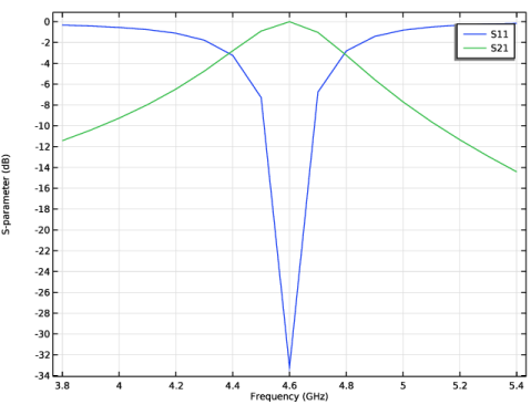
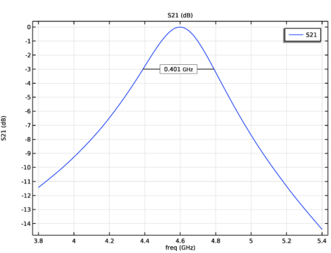
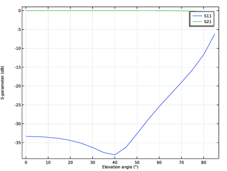
In the Settings window for Global, click Replace Expression in the upper-right corner of the y-Axis Data section. From the menu, choose Component 1 (comp1) > Electromagnetic Waves, Frequency Domain > Ports > S-parameter, dB - dB > emw.S21dB - S21.
Graph Marker 1
1
Right-click Global 1 and choose Graph Marker.
2
In the Settings window for Graph Marker, locate the Display section.
3
From the Display mode list, choose Bandwidth.
4
In the Cutoff value text field, type -3.
5
Locate the Text Format section. In the Precision text field, type 3.
6
Select the Include unit checkbox.
7
Click to expand the Coloring and Style section. Select the Show frame checkbox.